
In the ever-evolving world of semiconductor manufacturing, the relentless pursuit of smaller, faster, and more efficient devices hinges on perfection at the atomic level. As the industry pushes the boundaries of Moore’s Law, the purity of materials used in the process becomes critically important. One such material — the sputtering target — plays a central role in the thin film deposition processes used to fabricate integrated circuits, photovoltaic cells, and other high-tech devices.
While the base composition of a sputtering target is designed to achieve precise functional outcomes, it’s the trace impurities — often measured in parts per million (ppm) or even parts per billion (ppb) — that can spell the difference between a high-yield production run and costly semiconductor yield loss. In this article, we will explore how trace impurities in sputtering targets influence device yield, unravel the mechanisms behind defect formation, and discuss what manufacturers can do to mitigate these issues.
The Role of Sputtering Targets in Thin Film Deposition

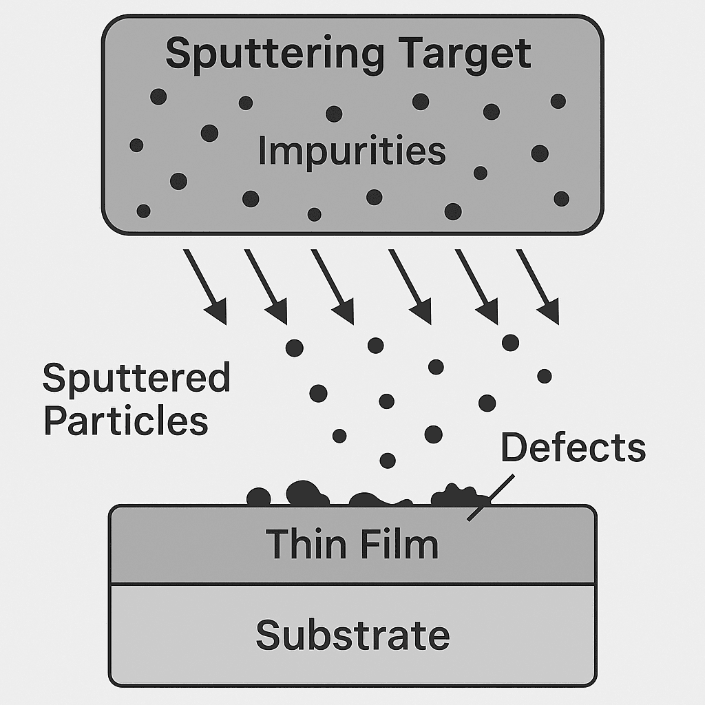
Sputtering targets are materials — typically metals, alloys, or ceramics — that are bombarded with ions in a vacuum chamber, causing atoms from the target to be ejected and deposited onto a substrate. This technique, known as physical vapor deposition (PVD), is widely used in producing thin films for semiconductors, optical coatings, magnetic storage, and advanced displays.
The performance and reliability of these thin films depend on the uniformity and purity of the sputtered material. Even minor compositional deviations or unwanted elements can lead to localized defects in the thin film, affecting electrical, optical, or magnetic properties.
Understanding Trace Impurities
Trace impurities refer to elements that are unintentionally present in the sputtering target. These impurities may arise from:
- Raw material contamination
- Processing equipment residues
- Environmental exposure during handling and packaging
Common trace metals such as iron (Fe), copper (Cu), nickel (Ni), and sodium (Na), even in ultra-low concentrations, can have a disproportionate impact on the final product, especially in high-sensitivity applications such as DRAM, NAND flash, or advanced logic devices.
Mechanisms by Which Impurities Affect Device Yield
1. Defect Formation in Thin Films
One of the most direct consequences of impurities in sputtering materials is the introduction of point defects and grain boundary irregularities in the deposited film. For example, a contaminant atom may substitute for a desired atom in the crystal lattice, distorting the structure and creating localized stress points. These defects can serve as nucleation sites for unwanted chemical reactions or reduce the crystallinity of the layer — a critical issue in gate dielectrics or tunnel oxides.
2. Electrical Leakage and Breakdown
In semiconductor devices, even minuscule amounts of metallic impurities can introduce trap states in the bandgap, increasing leakage currents and compromising device insulation. For instance, trace copper ions are notorious for migrating through oxide layers and causing premature dielectric breakdown. In logic devices, this can translate into performance degradation or total failure.
3. Corrosion and Reliability Issues
Certain impurities can catalyze corrosion under operational or storage conditions. For example, sodium contamination in sputtered films is known to promote electrochemical corrosion in TFT (thin-film transistor) displays and photovoltaic cells. Over time, this reduces the device’s operational lifetime, triggering early product recalls or warranty claims — scenarios that damage both revenue and reputation.
4. Unstable Film Growth
Impurities can alter the surface energy of the growing film, resulting in poor adhesion, variable film thickness, or columnar growth morphologies. This is particularly detrimental in applications requiring highly uniform coatings, such as hard disk platters or optical filters.
5. Process Inconsistencies and Particle Generation
Trace elements can oxidize or react differently during sputtering, generating micro-particles that contaminate wafers and cause killer defects. These microscopic particles, often invisible during initial inspection, can render entire wafers unusable. High-purity sputtering targets help maintain stable plasma conditions and reduce such particulate contamination.
Real-World Impact on Semiconductor Yields
Yield loss in semiconductor manufacturing is often attributed to a complex interplay of factors — including photolithography misalignments, etch errors, and dopant diffusion — but material purity stands as a quiet, often overlooked culprit.
Consider this: In a typical 300mm wafer fabrication process, a defect density of just one particle per square centimeter can result in catastrophic die loss. When yields are measured in microns and defects in atoms, trace metals in sputtering targets can no longer be considered benign.
In high-volume manufacturing (HVM), even a 0.1% yield improvement can translate to millions of dollars in savings. Hence, companies are now investing heavily in ultra-high purity (UHP) sputtering targets with certified impurity levels below 1 ppm for critical elements. This shift is not merely precautionary — it’s economically imperative.
Trace Impurity Analysis Techniques
Glow Discharge Mass Spectrometry (GDMS)
GDMS is among the most sensitive techniques for detecting trace impurities in solid materials. It provides multi-element detection capabilities down to ppb levels and is routinely used for quality assurance of sputtering targets.
Inductively Coupled Plasma Mass Spectrometry (ICP-MS)
For a more detailed elemental breakdown, ICP-MS offers high precision and is ideal for analyzing the raw powders or metallic melts used in target fabrication.
X-Ray Fluorescence (XRF)
Though less sensitive than GDMS or ICP-MS, XRF is useful for quick surface screening and verifying compositional homogeneity.
Manufacturers now often provide full certificates of analysis (CoAs) with these data points to assure customers of sputtering target purity.
Mitigation Strategies for Impurity Control
To minimize the impact of trace impurities, leading sputtering target suppliers employ a combination of the following techniques:
1. Source Purity Control
High-purity starting materials are non-negotiable. Vendors typically use 5N (99.999%) or higher purity base elements. For semiconductors, 6N and 7N purities are becoming the norm, especially for elements like tantalum, titanium, and molybdenum.
2. Vacuum Melting and Refining
Techniques such as vacuum arc melting (VAM) and electron beam melting (EBM) help reduce volatile impurities and produce a cleaner microstructure.
3. Hot Isostatic Pressing (HIP)
HIP improves density and eliminates internal porosity, which can otherwise harbor contaminants. It also helps achieve uniform grain size distribution, further reducing the risk of impurity-induced defects.
4. Cleanroom Handling and Packaging
To prevent post-production contamination, targets are handled in ISO class 5 or better cleanroom environments and are vacuum-sealed with desiccants or inert gas backfill.
Industry Trends and Future Outlook
As device architectures move toward 3D integration, gate-all-around (GAA) FETs, and advanced packaging, the tolerance for process-induced variability shrinks dramatically. The demand for low-defect-density thin films continues to grow.
In response, target manufacturers are exploring innovations such as:
- Zone-refined materials
- AI-driven process control for impurity prediction
- Advanced recycling with impurity filtration
Moreover, eco-conscious production is gaining traction, with companies seeking to reduce the carbon footprint of sputtering target manufacturing while maintaining ultra-purity levels — a dual challenge that underscores the complexity of modern materials science.
FAQs: How Trace Impurities in Sputtering Targets Affect Device Yield
1. What are trace impurities in sputtering targets?
Trace impurities are unintended elements or compounds present in sputtering targets, typically in parts per million (ppm) or parts per billion (ppb) concentrations. These can originate from raw materials, manufacturing equipment, or environmental contamination.
2. Why is sputtering target purity important for semiconductor manufacturing?
High purity is crucial because even tiny amounts of contaminants can lead to defects in thin films, such as electrical leakage, grain boundary abnormalities, or particle generation — all of which reduce device yield.
3. What are the most common trace contaminants in sputtering materials?
Iron (Fe), Copper (Cu), Sodium (Na), Nickel (Ni), and Carbon (C) are among the most common impurities found in sputtering targets that can affect thin film properties.
4. How do trace metals affect thin film deposition?
They can cause point defects, alter the film’s electrical and optical characteristics, generate particles during sputtering, and affect adhesion or crystallinity of the deposited film.
5. Can impurities cause semiconductor yield loss directly?
Yes. Contaminants can lead to short circuits, dielectric breakdown, leakage current, and corrosion, directly reducing functional yield in wafer fabrication.
6. What techniques are used to detect trace impurities in sputtering targets?
Analytical methods like Glow Discharge Mass Spectrometry (GDMS), Inductively Coupled Plasma Mass Spectrometry (ICP-MS), and X-Ray Fluorescence (XRF) are commonly used to identify and quantify trace elements.
7. What purity levels are considered acceptable for sputtering targets used in semiconductors?
Ultra-high purity targets typically range from 99.99% (4N) to 99.9999% (6N), depending on the application. For advanced nodes, targets with total metallic impurities <1 ppm are preferred.
8. How can manufacturers reduce the risk of impurities in sputtering targets?
By using ultra-pure raw materials, adopting vacuum melting and hot isostatic pressing (HIP), and maintaining strict cleanroom standards during processing and packaging.
9. Do all applications require ultra-pure sputtering targets?
Not necessarily. High-end semiconductor and optoelectronic applications demand the highest purity, while industrial coatings or some magnetic films may tolerate slightly lower grades.
10. Where can I source high-purity sputtering targets for thin film deposition?
Reputable suppliers like TFM (Thin Film Materials) offer high-purity sputtering targets with certified low impurity levels, ideal for demanding vacuum coating and semiconductor applications.
Conclusion
The science of sputtering is, at its heart, the art of precision. In a world where a single atom out of place can ruin a million-dollar wafer, the presence of trace impurities in sputtering targets is far from trivial.
From inducing point defects and electrical failures to affecting film uniformity and long-term reliability, these microscopic contaminants exert a macroscopic influence on device yield. As semiconductor nodes continue to shrink and functional demands soar, the purity of sputtering targets will remain a cornerstone of success in thin film deposition and vacuum coating technologies.
By investing in ultra-high purity targets, leveraging advanced analytical techniques, and maintaining rigorous process controls, manufacturers can significantly enhance their yields, reduce waste, and uphold the performance promises of modern microelectronics.
In the end, it’s not just about making devices work — it’s about making them work flawlessly, reliably, and profitably.