Generic selectors
Exact matches only
Search in title
Search in content
Post Type Selectors

Semiconductor Substrates – Materials, Properties, and Applications

This article provides an in-depth exploration of various semiconductor substrates, including silicon, indium arsenide, gallium arsenide, gallium antimonide, indium phosphide, thermal oxide silicon, and polysilicon wafers. It covers their physical properties, manufacturing processes, and key applications in integrated circuits, high-frequency electronics, and optoelectronic devices. The article also compares the advantages and limitations of each substrate and discusses future trends and innovations, offering a comprehensive understanding of the critical role substrates play in modern electronics technology.

Table of Contents

Chapter 1

1. Introduction to Semiconductor Substrates
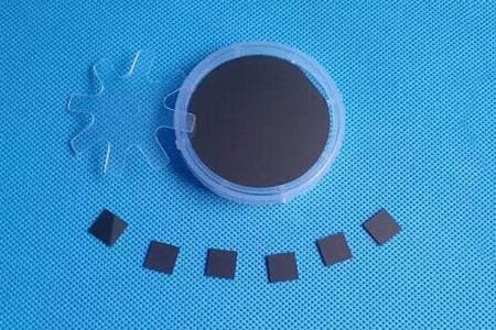
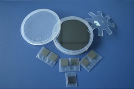
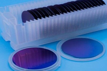
Semiconductor substrates serve as the essential foundation of virtually all modern electronic and optoelectronic devices. Without these substrates, the intricate structures of transistors, diodes, sensors, and lasers could not be constructed. Fundamentally, a semiconductor substrate is a wafer—typically a thin slice of semiconductor material—on which multiple layers of materials and circuits are fabricated through processes such as doping, deposition, etching, and lithography.

The choice of substrate profoundly influences device performance, manufacturing complexity, and cost. As the backbone of semiconductor devices, substrates must provide excellent mechanical stability, thermal conductivity, and, importantly, appropriate electronic properties such as crystal quality and lattice constant compatibility with epitaxial layers. Historically, silicon wafers have been the substrate of choice for decades, driven by their abundance, mature processing technologies, and excellent electrical characteristics. However, the demand for higher performance, faster operation, and new functionalities has encouraged the adoption of a broader range of semiconductor substrates, especially compound semiconductors.

In this comprehensive overview, we will explore the key semiconductor substrates currently used in industry and research, such as Silicon (Si), Indium Arsenide (InAs), Gallium Arsenide (GaAs), Gallium Antimonide (GaSb), Indium Phosphide (InP), Thermal Oxide Silicon Wafers, and Polysilicon Wafers. We will detail their material properties, manufacturing methods, advantages, and specific applications, providing a holistic understanding of their roles in advancing technology.

Chapter 2

2. Silicon Wafer (Si)

Historical Context and Dominance

Silicon has been the workhorse of the semiconductor industry since the invention of the transistor in the late 1940s. Its unique combination of abundance, low cost, and semiconductor properties quickly established it as the dominant substrate material. The mass production and refinement of silicon wafers accelerated with the invention of the Czochralski crystal growth technique in the 1950s, enabling large, high-purity, single-crystal ingots.

Material Properties and Electrical Behavior

Silicon is a group IV element with an indirect bandgap of approximately 1.12 eV at room temperature. The indirect bandgap means that photons are not efficiently emitted or absorbed, which limits silicon’s use in optoelectronics but excels in electronic applications. Silicon’s thermal conductivity (about 149 W/m·K) helps dissipate heat generated during device operation, essential for maintaining performance and reliability.Its mechanical strength allows for wafer thinning, essential in modern packaging and integration techniques. The lattice constant of silicon is well-matched to many silicon-based compounds, enabling high-quality epitaxial layers crucial for advanced CMOS (complementary metal-oxide-semiconductor) technologies.

Manufacturing: From Ingot to Wafer

Silicon wafers begin as high-purity polysilicon, melted in a crucible and grown into single-crystal cylindrical ingots using the Czochralski or float-zone processes. The diameter of these ingots determines the wafer size; currently, 300 mm wafers are standard in production, with 450 mm under development.The ingots are sliced using wire saws into thin wafers, which then undergo surface polishing and chemical-mechanical planarization to achieve atomically smooth surfaces, essential for lithographic patterning. Silicon wafers can be doped during or after growth to tailor electrical properties for device needs.

Types of Silicon Wafers

  • Monocrystalline Silicon: Single-crystal wafers with uniform crystallographic orientation, used for high-performance integrated circuits and power devices.

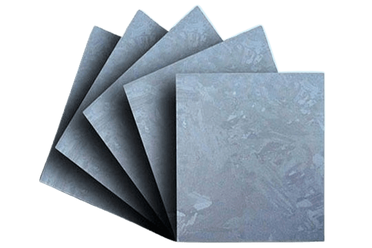
  • Multicrystalline Silicon: Wafers composed of multiple smaller crystals; less expensive but with lower electronic quality. Predominantly used in solar photovoltaics.

  • Silicon-on-Insulator (SOI): Wafers with a thin insulating layer (usually silicon dioxide) beneath a top silicon layer, improving device speed and reducing parasitic capacitance.

Applications

Silicon wafers are ubiquitous in microprocessors, memory chips, power electronics, sensors, and photovoltaic solar cells. The maturity of silicon technology has enabled the miniaturization of electronics, following Moore’s Law for decades. Additionally, silicon’s compatibility with thermal oxide layers forms the basis of MOSFET transistors, the building blocks of digital logic.

Chapter 3

3. Indium Arsenide Wafer (InAs)

Material Characteristics

Indium Arsenide, a III-V compound semiconductor, offers unique electronic properties that differentiate it from silicon. It has a very narrow direct bandgap of approximately 0.36 eV at room temperature, enabling high absorption in the infrared spectrum. Additionally, InAs exhibits electron mobilities reaching as high as 30,000 cm²/Vs, dramatically higher than silicon’s typical 1400 cm²/Vs.

This exceptionally high electron mobility allows for ultra-fast electronic devices with low power dissipation, making InAs a critical material for specialized high-frequency and optoelectronic applications.

Manufacturing Challenges

The production of InAs wafers is complex and costly. Growth techniques such as molecular beam epitaxy (MBE) and metal-organic chemical vapor deposition (MOCVD) enable precise control of stoichiometry and crystal quality but require ultra-high vacuum and sophisticated equipment. The relatively large lattice constant (~6.06 Å) makes it challenging to grow high-quality layers on dissimilar substrates without inducing defects.Moreover, InAs substrates are brittle and sensitive to handling, increasing manufacturing difficulty.

Applications

Due to its narrow bandgap and high electron mobility, InAs is widely used in infrared detectors, such as those used for thermal imaging, night vision, and gas sensing. Quantum dot lasers and high-electron-mobility transistors (HEMTs) for microwave and millimeter-wave communications also rely on InAs.

Its potential in quantum computing as a platform for topological qubits is currently an area of active research, highlighting InAs’s emerging importance beyond traditional electronics.

Chapter 4

4. Gallium Arsenide Wafer (GaAs)

Material Advantages over Silicon

Gallium Arsenide (GaAs) is another III-V compound semiconductor known for its direct bandgap of approximately 1.42 eV, making it highly efficient for optoelectronic emission and detection. The direct bandgap facilitates the emission of light, a property silicon lacks due to its indirect bandgap.The electron mobility in GaAs (~8500 cm²/Vs) is significantly higher than silicon, enabling transistors to switch faster and operate at higher frequencies. This makes GaAs the substrate of choice for RF (radio frequency) and microwave applications.

Manufacturing and Wafer Quality

GaAs wafers are grown using methods such as liquid encapsulated Czochralski (LEC) and vertical gradient freeze (VGF), which produce high-purity, single-crystal wafers with minimal defects. Wafer diameters typically range from 2 to 6 inches, smaller than silicon wafers, mainly due to growth constraints.Surface preparation and polishing techniques have been refined to ensure smoothness compatible with advanced epitaxy and device fabrication.

Applications in Optoelectronics and RF

GaAs’s direct bandgap makes it ideal for LEDs, laser diodes, and solar cells, particularly in high-efficiency, radiation-hard space applications. GaAs solar cells outperform silicon cells in harsh environments due to better radiation resistance and efficiency at high temperatures.In telecommunications, GaAs substrates are used for high-speed transistors in cell phones, satellite communication, and radar systems. GaAs high electron mobility transistors (HEMTs) are critical for amplifiers and mixers operating at microwave and millimeter-wave frequencies.

Chapter 5

5. Gallium Antimonide Wafer (GaSb)

Unique Material Properties

Gallium Antimonide (GaSb) is a III-V semiconductor with a narrow direct bandgap of about 0.726 eV, placing it in the infrared spectrum. GaSb exhibits high hole mobility, a desirable property for p-type transistors and certain photodetectors.Its lattice constant (~6.1 Å) makes GaSb compatible with other antimonide materials, enabling complex heterostructures for novel devices.

Growth and Processing Challenges

GaSb crystal growth is more challenging than GaAs or silicon, requiring precise temperature control and stoichiometry management to minimize defects. Advanced epitaxial methods, including molecular beam epitaxy (MBE), have allowed the development of high-quality GaSb substrates.

Applications in Infrared and Thermophotovoltaics

GaSb substrates are critical in mid-infrared photodetectors used for gas sensing, environmental monitoring, and medical diagnostics. Its bandgap aligns with the absorption spectrum of many gases, enabling sensitive detection.In thermophotovoltaics, GaSb-based devices convert heat radiation directly into electricity with high efficiency, promising applications in waste heat recovery and portable power generation.

Chapter 6

6. Indium Phosphide Wafer (InP)

Applications in Infrared and Thermophotovoltaics

GaSb substrates are critical in mid-infrared photodetectors used for gas sensing, environmental monitoring, and medical diagnostics. Its bandgap aligns with the absorption spectrum of many gases, enabling sensitive detection.In thermophotovoltaics, GaSb-based devices convert heat radiation directly into electricity with high efficiency, promising applications in waste heat recovery and portable power generation.

Manufacturing Techniques

InP wafers are produced mainly through the vertical gradient freeze (VGF) method, resulting in large single crystals with high purity. The wafers are available in diameters typically between 2 and 6 inches, with surface treatments optimizing epitaxy.

Applications in Photonics and Communications

InP substrates are the backbone of fiber optic communications, used to fabricate laser diodes, modulators, and photodetectors with wavelengths compatible with optical fiber transmission windows (1.3 and 1.55 microns).High-frequency transistors fabricated on InP substrates serve in radar, satellite communications, and emerging 5G technologies. The substrate’s properties facilitate photonic integrated circuits, combining optical and electronic functions on a single chip.

Chapter 7

7. Thermal Oxide Silicon Wafers (Si + SiO₂)

Importance of Thermal Oxide Layers

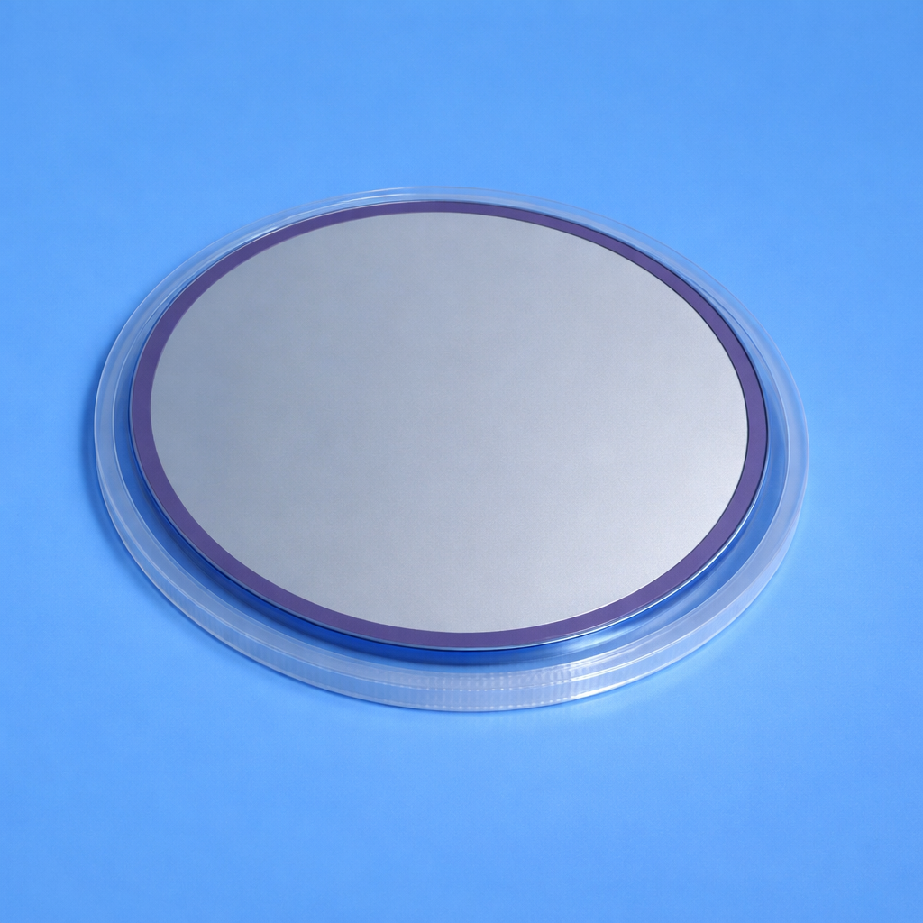
Thermal oxide silicon wafers involve the growth of a silicon dioxide (SiO₂) layer on silicon substrates by high-temperature oxidation. This SiO₂ layer serves as a high-quality insulator and a key component in MOS (metal-oxide-semiconductor) devices.The interface quality between silicon and the thermal oxide determines device reliability, leakage currents, and gate control.

Process and Control

Thermal oxidation involves exposing silicon wafers to oxygen or steam at temperatures typically between 900°C and 1200°C. The oxide thickness can be precisely controlled by oxidation time and temperature, allowing oxide layers from a few nanometers to microns.Advancements in oxidation techniques, such as dry, wet, and rapid thermal oxidation, enable tailoring of oxide properties for different applications.

Applications in CMOS and Sensors

Thermally grown oxide layers form the gate dielectric in CMOS transistors, the most widely used device in modern electronics. The quality of this oxide determines transistor switching speed, power consumption, and reliability.In MEMS and sensor technologies, thermal oxide layers provide electrical isolation and chemical stability, enabling integration of electronic and mechanical functions.

Chapter 8

8. Polysilicon (Multicrystalline) Wafer

Structural Characteristics

Polysilicon wafers consist of many small silicon crystals or grains, separated by grain boundaries that act as recombination centers for charge carriers. This structural difference makes polysilicon less efficient electronically than monocrystalline silicon.

Advantages and Cost

Despite lower electronic performance, polysilicon wafers are cheaper to produce and can be fabricated in larger sizes. The polycrystalline structure allows for simplified manufacturing processes without the need for perfect crystal alignment.

Applications in Solar Cells and Large-Area Electronics

Polysilicon wafers dominate the solar photovoltaic industry, where cost per watt is more critical than maximum efficiency. Techniques such as surface passivation and selective doping have improved the efficiency of polysilicon solar cells, narrowing the gap with monocrystalline cells.Large-area thin-film transistors (TFTs) for displays also utilize polysilicon films due to their cost-effectiveness.

Chapter 9

9. Comparative Analysis of Substrates

Choosing a semiconductor substrate depends on many factors: electrical properties, lattice matching, thermal conductivity, cost, and application requirements. Silicon remains the go-to for mainstream microelectronics due to its balance of cost and performance. III-V substrates like GaAs and InP excel in high-frequency and optoelectronic applications but come with higher costs and manufacturing challenges.

A comparison of key properties is summarized in the table below:

SubstrateBandgap (eV)Electron Mobility (cm²/Vs)Thermal Conductivity (W/m·K)Typical Wafer SizeKey ApplicationsCost
Silicon (Si)1.12 (indirect)~1400~149200-300 mmMicroprocessors, sensors, solar cellsLow
Indium Arsenide (InAs)0.36 (direct)~30,000~272-3 inchIR detectors, quantum devicesHigh
Gallium Arsenide (GaAs)1.42 (direct)~8500~462-6 inchRF devices, LEDs, solar cellsHigh
Gallium Antimonide (GaSb)0.726 (direct)Moderate~332-3 inchIR sensors, thermophotovoltaicsHigh
Indium Phosphide (InP)1.34 (direct)High~682-6 inchFiber optics, photonicsHigh
Thermal Oxide SiSi + SiO₂N/AN/A200-300 mmCMOS, sensorsModerate
Polysilicon1.12Lower than monocrystal~140150-200 mmSolar panels, TFTsLow

Chapter 10

10. Future Trends and Innovations

The semiconductor substrate landscape is evolving rapidly, driven by the demand for faster, smaller, and more energy-efficient devices. Emerging materials such as silicon carbide (SiC) and gallium nitride (GaN) are gaining traction, especially in power electronics and RF applications, due to their wide bandgaps and superior thermal properties.

Wafer diameters continue to increase, enabling economies of scale but requiring innovations in crystal growth and wafer handling. The push toward 450 mm silicon wafers exemplifies this trend, though the transition poses significant engineering challenges.

New substrate technologies like flexible electronics demand bendable and stretchable materials, sometimes integrating semiconductor thin films on plastic or metal foils. Two-dimensional materials, such as graphene and transition metal dichalcogenides (TMDs), also represent future substrates that could revolutionize device architectures.

Quantum computing and spintronics introduce additional substrate requirements, emphasizing ultra-high purity and defect control, opening new frontiers in substrate engineering.


Chapter 11

Frequently Asked Questions (FAQs)

Powder metallurgy offers several benefits, including cost-effective production, the ability to create complex shapes, tight and uniform tolerances, excellent surface finishes, lower material waste, energy-efficient processes, and the ability to work with unique materials.

Future advancements are likely to include the development of nanostructured powders, further integration of machine learning for process optimization, enhanced sustainable manufacturing practices, and expanded applications in additive manufacturing. These innovations will continue to improve the performance, consistency, and cost-effectiveness of alloy powders in high-performance sectors.

Chapter 12

Conclusion

Semiconductor substrates are the critical starting point for all electronic and photonic devices. From the ubiquitous silicon wafer to the specialized III-V compound wafers like GaAs, InAs, and InP, each substrate offers unique advantages that make it suitable for specific applications. The interplay of material properties, manufacturing methods, and cost considerations shapes the global semiconductor industry.Understanding the nuances of these substrates empowers engineers and researchers to select the best platform for their devices, whether for everyday computing, high-speed communications, or cutting-edge sensing technologies. As technology advances, innovations in substrate materials and manufacturing will continue to drive the evolution of electronics, ensuring substrates remain foundational to the future of technology.
Shopping Cart
Scroll to Top