If you work in industries like electronics, aerospace, or optics, you likely know how crucial it is to have a reliable thin film deposition process. Thin films are used in a wide variety of applications, from electronic components to optical coatings, and ensuring the quality of these films can make a significant difference in product performance. One of the most popular and versatile methods for thin film deposition is e-beam evaporation (electron beam evaporation).
In this comprehensive guide, we’ll explore the principles of e-beam evaporation, its advantages and limitations, the essential components of an e-beam evaporation system, and various techniques to optimize thin film deposition. Whether you’re a newcomer to thin film technologies or an experienced practitioner, this guide will help you understand how to take your thin film deposition process to the next level.
Understanding Thin Film Deposition
What is Thin Film Deposition?
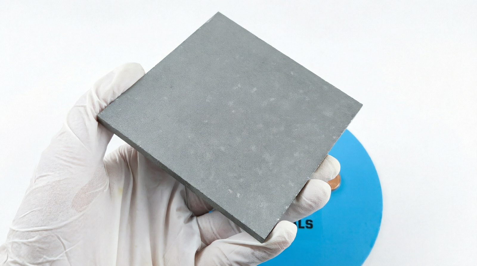
Thin film deposition is the process of applying a thin layer of material onto a substrate. These layers can be just a few nanometers thick or several micrometers, depending on the application. Thin films are used in a wide array of industries, including electronics, optics, energy, and aerospace.
There are several deposition techniques, including:
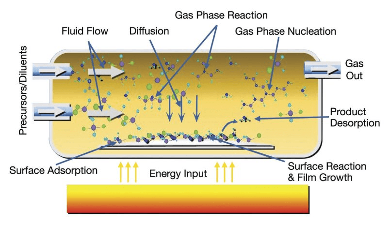
- Physical Vapor Deposition (PVD): A category of deposition methods where material is vaporized and transported to the substrate in a vacuum environment.
- Chemical Vapor Deposition (CVD): A process where gaseous chemical precursors react to deposit material on a substrate.
- Electron Beam (E-Beam) Evaporation: A form of PVD that uses an electron beam to heat and vaporize material, which then condenses on the substrate.
In e-beam evaporation, the process is conducted under high vacuum conditions to avoid contamination, ensuring that the thin film is as pure and uniform as possible.
Principles of E-Beam Evaporation
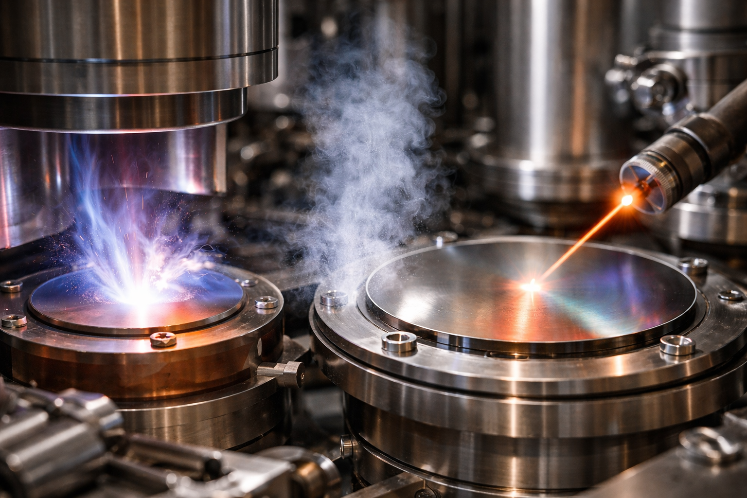
E-beam evaporation works by focusing a high-energy electron beam on a target material, typically in a vacuum chamber. This electron beam generates sufficient energy to vaporize the material, which is then transported to the substrate, where it condenses and forms a thin film. The process is effective for a wide variety of materials, including metals, semiconductors, and insulators.
Because the process occurs in a vacuum, there is minimal contamination, and the resulting films are highly pure. The ability to control the energy and focus of the electron beam makes e-beam evaporation ideal for creating thin films with high uniformity and precision.
Advantages of E-Beam Evaporation
1. Wide Material Compatibility
E-beam evaporation is capable of depositing a broad range of materials, including metals like gold, aluminum, and copper, as well as semiconductors such as silicon and germanium, and even insulators like silicon dioxide and titanium dioxide. This makes it a versatile technique for industries like electronics, aerospace, and optics, where diverse materials are needed.
2. High Purity and Uniformity
One of the main advantages of e-beam evaporation is its ability to produce thin films with exceptional purity and uniformity. Since the deposition occurs under high vacuum conditions, the material is less likely to be contaminated during the process. This is crucial for applications where thin films must meet strict quality standards, such as in electronics and semiconductors.
3. Control over Film Thickness
The e-beam evaporation process offers precise control over the deposition rate and film thickness. By adjusting the energy of the electron beam and controlling the distance between the electron gun and the substrate, operators can produce films with highly accurate thicknesses.
4. Ability to Deposit High Melting Point Materials
E-beam evaporation is particularly effective for materials with high melting points, such as tungsten and molybdenum, which are commonly used in aerospace and electronics industries. These materials can be vaporized and deposited onto substrates without the need for extremely high temperatures, which might be required in other deposition methods like thermal evaporation.
Limitations of E-Beam Evaporation
1. Limited Deposition Area
The electron beam in e-beam evaporation is typically focused on a small spot on the source material. This limitation means that the deposition area is constrained, making it more challenging to coat large substrates efficiently. However, this can be mitigated by using multiple electron guns or rotating the substrate during the process.
2. Potential for Source Material Damage
The high-energy electron beam used in e-beam evaporation can cause thermal damage to the source material. This is because the beam rapidly heats up the material, which can lead to overheating or evaporation of the source material if not properly managed. Careful attention must be paid to the energy settings of the electron beam to avoid such issues.
3. Complex Setup
Setting up and operating an e-beam evaporation system can be more complex compared to other deposition techniques. The vacuum chamber needs to be maintained at a high level of cleanliness, and precise control of the electron gun and substrate holder is required to ensure consistent deposition.
The E-Beam Evaporation System: Key Components
An e-beam evaporation system is composed of several key components, each playing a crucial role in ensuring efficient and accurate deposition.
1. Electron Gun
The electron gun is the heart of the e-beam evaporation system. It generates the high-energy electron beam that heats and vaporizes the source material. The electron gun typically consists of a cathode, anode, and heated filament. The electron beam is focused onto the source material, where it provides the energy necessary for vaporization.
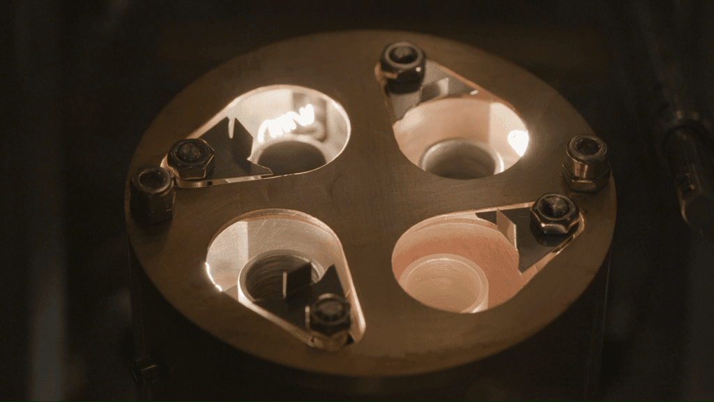
2. Crucible
The crucible holds the source material. Made from a heat-resistant material (like a tungsten or molybdenum), the crucible ensures that the source material is heated efficiently without contamination. The electron beam is directed at the crucible to vaporize the material, which then condenses on the substrate.
3. Substrate Holder
The substrate holder holds the substrate in place during deposition. This component is essential for ensuring that the vaporized material condenses onto the substrate in a controlled manner. The substrate holder can be rotated or tilted to ensure uniform deposition across the surface of the substrate.
4. Vacuum Chamber
The vacuum chamber is where the entire e-beam evaporation process takes place. It is essential for maintaining the high vacuum conditions needed to prevent contamination during deposition. The vacuum chamber typically maintains a pressure of around 10^-6 torr to ensure that the vaporized material travels cleanly to the substrate without interacting with unwanted gases or particles.
E-Beam Evaporation Techniques
1. Direct Deposition
In direct deposition, the electron beam is focused directly on the source material, causing it to vaporize. The vaporized material then condenses onto the substrate, forming a thin film. This is the most straightforward technique for e-beam evaporation.
2. Shutter-Controlled Deposition
A shutter can be used between the crucible and the substrate holder to regulate the amount of vapor that reaches the substrate. By opening and closing the shutter, the deposition rate can be controlled, allowing for precise management of film thickness.
3. Co-Evaporation
In co-evaporation, two or more materials are vaporized simultaneously to form a composite thin film. This technique is used to create alloys or other multi-material films with specific properties, such as those required in semiconductor or optical applications.
Materials Used in E-Beam Evaporation
E-beam evaporation can be used to deposit a wide range of materials, including:
- Metals: Gold, silver, copper, titanium, tungsten, and aluminum
- Semiconductors: Silicon, germanium, gallium arsenide
- Insulators: Silicon dioxide, titanium dioxide
The choice of material depends on the desired properties of the thin film, such as electrical conductivity, optical transparency, or mechanical durability.
Factors Affecting E-Beam Evaporation Efficiency
Several factors influence the efficiency of the e-beam evaporation process, including:
- Deposition Rate: Controlled by electron beam power, crucible size, and distance between the electron gun and the crucible.
- Deposition Angle: Affected by the distance between the substrate and the crucible, as well as the positioning of the substrate holder.
- Substrate Temperature: Affects film adhesion and crystallinity. Higher temperatures can promote better adhesion but may also cause stress in the film.
Applications of E-Beam Evaporation
E-beam evaporation is used in various industries for the deposition of thin films. Some key applications include:
1. Electronics
In the electronics industry, e-beam evaporation is used to deposit thin films of metals and semiconductors on substrates to create electronic components such as transistors, diodes, and integrated circuits.
2. Optics
E-beam evaporation is also used in the optics industry to create components like mirrors, lenses, and optical coatings by depositing thin films of metals and dielectric materials on substrates.
3. Aerospace
The aerospace industry benefits from e-beam evaporation for the deposition of thin films on components used in satellites, spacecraft, and other high-performance applications. Materials such as tungsten and molybdenum are often used in aerospace components.
Comparing E-Beam Evaporation with Other Deposition Methods
While e-beam evaporation is highly effective, it is important to consider other deposition techniques such as sputtering, thermal evaporation, and chemical vapor deposition (CVD). Each method has its advantages and limitations, depending on the specific requirements of the application.
- Sputtering: Involves bombarding a target material with ions to release atoms, which then condense onto the substrate.
- Thermal Evaporation: Involves heating the source material to evaporate it, without the use of an electron beam.
- CVD: Involves chemical reactions to deposit thin films from gaseous precursors.
Each technique has its strengths, such as sputtering’s ability to cover larger areas or CVD’s ability to produce complex films. The choice of technique will depend on factors like film properties, deposition speed, and material compatibility.
Conclusion
E-beam evaporation is a versatile and highly effective method for thin film deposition, offering benefits such as high purity, uniformity, and the ability to deposit a wide range of materials. While it has some limitations, such as restricted deposition area and potential source material damage, it remains a popular choice in industries like electronics, optics, and aerospace.
By understanding the fundamentals of e-beam evaporation, its key components, techniques, and materials, you can optimize your thin film deposition process to achieve superior results. Whether you are just starting or looking to refine your skills, e-beam evaporation can help you create thin films with exceptional quality and precision.