Indium is a unique and highly valued metal known for its low melting point, malleability, and excellent adhesive properties. These characteristics make it an essential material in advanced technologies, particularly in the creation of thin-film coatings and semiconductor devices. Evaporating indium is a fundamental process used to create precise, uniform coatings in a variety of industrial and scientific applications. This article explores the process in detail, focusing on the scientific principles, technical requirements, challenges, and applications of indium evaporation.
Understanding Indium and Its Characteristics
Indium, a post-transition metal found in Group 13 of the periodic table, is recognized for its remarkable softness and ductility. Its low melting point of 156.6°C and boiling point of approximately 2072°C make it suitable for evaporation techniques, which rely on transforming a material into vapor under controlled conditions. Indium’s high affinity for oxygen, however, poses challenges, as it can readily form indium oxide when exposed to air, potentially compromising the quality of the evaporation process.
The motivation to evaporate indium lies in its critical role in creating thin films for cutting-edge applications. These films are vital in manufacturing components such as touchscreens, solar panels, and high-speed semiconductors. Evaporation allows for precise control over the thickness and uniformity of the deposited indium layer, ensuring optimal performance in these applications.
The Science of Indium Evaporation
Evaporation is a process in which a material transitions from a solid or liquid state to a vapor state by heating it to its boiling point. In the context of indium, this process is typically carried out in a vacuum environment to reduce contamination and minimize the temperature required for evaporation. The vacuum creates low-pressure conditions, allowing indium to vaporize at a lower temperature than it would at atmospheric pressure.
The choice of heating method plays a crucial role in the efficiency and precision of the evaporation process. Resistive heating is a straightforward technique where electric current heats a crucible containing indium, gradually turning it into vapor. Alternatively, electron beam (e-beam) evaporation uses a focused electron beam to heat the indium target directly. This method provides superior control, enabling the deposition of ultra-thin and uniform layers, particularly useful for advanced scientific research and semiconductor manufacturing.
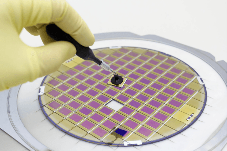
Setting Up the Evaporation Process
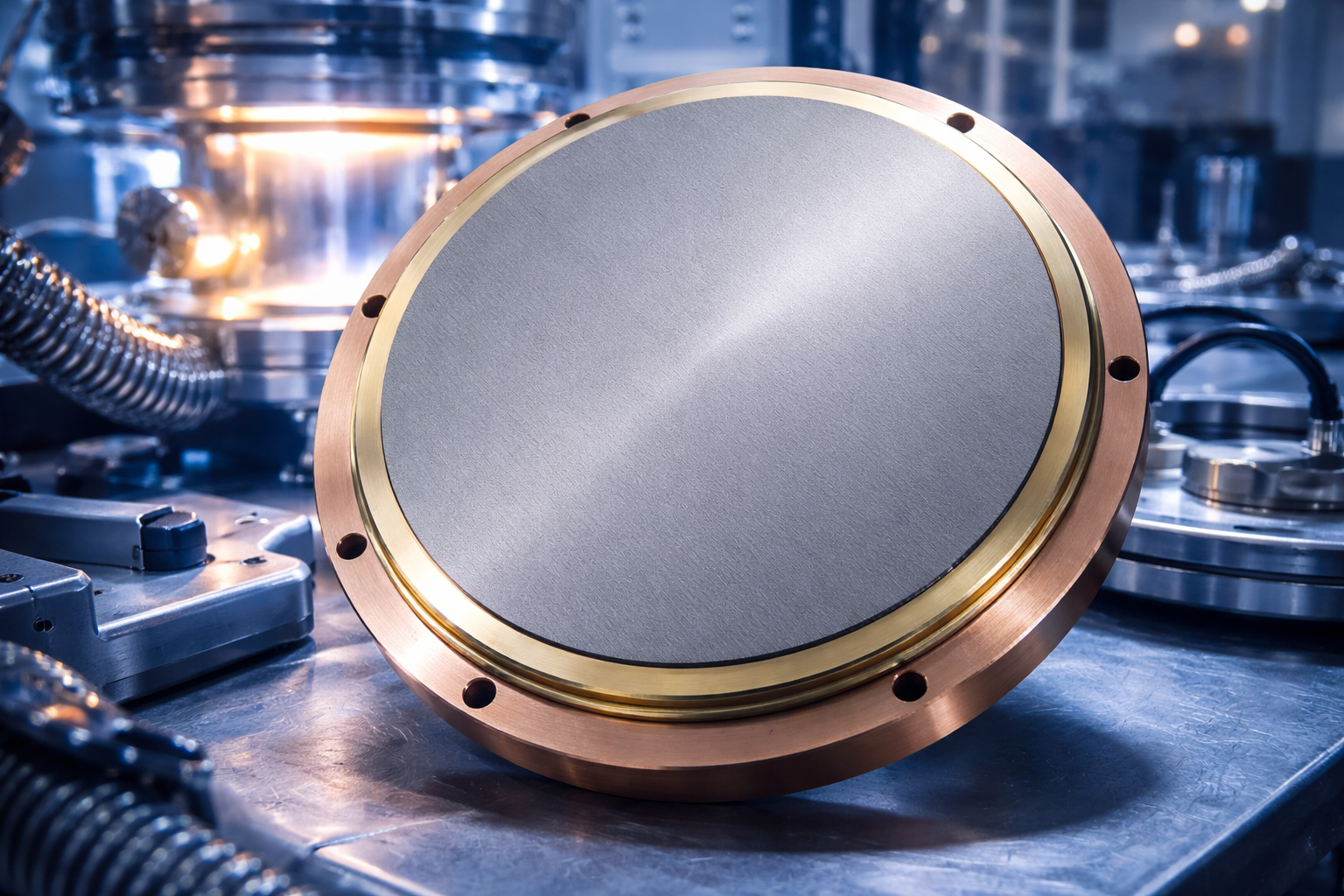
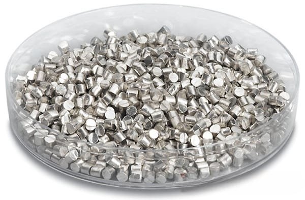
The process begins with careful preparation of the indium and the vacuum chamber. High-purity indium is essential to avoid introducing impurities into the final film. The metal is typically prepared in pellet or wire form, which allows for easier handling and consistent vaporization. The vacuum chamber must be meticulously cleaned to eliminate contaminants that could interfere with the deposition process.
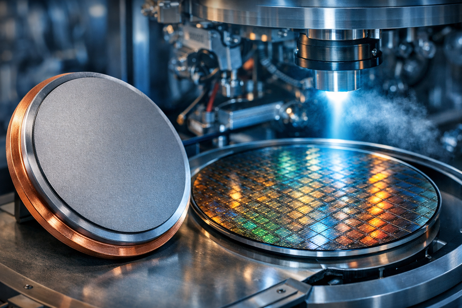
Once the indium and substrates are placed inside the chamber, vacuum pumps are used to achieve the required low-pressure environment, often reaching levels as low as 10−610^{-6}10−6 to 10−810^{-8}10−8 Torr. This ensures that the evaporation process occurs in a highly controlled atmosphere, free from oxygen and other reactive gases.
Temperature control is critical during evaporation. The heating process begins gradually to melt the indium without causing spattering or uneven vaporization. Real-time monitoring systems, such as quartz crystal microbalances (QCM), are used to measure the rate of deposition and the thickness of the indium film. These tools ensure that the film is deposited with the precision required for specific applications.
Challenges in Indium Evaporation
Evaporating indium is not without its difficulties. One of the most significant challenges is managing its tendency to oxidize when exposed to air. Even trace amounts of oxygen in the vacuum chamber can lead to the formation of indium oxide, compromising the quality of the deposited film. To address this, ultra-high vacuum (UHV) conditions are often employed, and inert gases like argon may be introduced to displace residual oxygen.
Another challenge is the risk of contamination from impurities in the indium or the evaporation system itself. High-purity materials and rigorous cleaning protocols are essential to minimize this risk. Furthermore, indium’s low melting point can make it prone to spattering if overheated, resulting in non-uniform films. Careful control of the heating rate and temperature is necessary to avoid these issues.
Thermal management also plays a pivotal role in the evaporation process. Indium’s properties require precise adjustments to the heating system to achieve a consistent vaporization rate. Advanced equipment, such as e-beam evaporators, offers the level of precision needed to overcome these challenges, making them a preferred choice for high-stakes applications.
Applications of Indium Evaporation
The thin films created through indium evaporation are integral to a wide range of modern technologies. One prominent application is in the field of optoelectronics, where indium-tin oxide (ITO) films are used as transparent conductive coatings in devices like touchscreens, flat-panel displays, and photovoltaic cells. The uniformity and conductivity of these coatings are directly influenced by the evaporation process.
In the semiconductor industry, indium plays a crucial role in the development of high-speed electronic devices. Compound semiconductors, such as indium phosphide (InP) and indium gallium arsenide (InGaAs), are pivotal for applications in telecommunications and infrared sensing. Evaporation enables the precise deposition of these materials, ensuring the performance and reliability of the resulting devices.
Indium films are also used in the creation of optical coatings, including anti-reflective and reflective layers for lenses and other optical components. The ability to produce thin, uniform layers is essential for achieving the desired optical properties. Beyond industrial applications, indium evaporation is a valuable tool in scientific research, facilitating the study of thin-film properties and the development of novel materials.
The Future of Indium Evaporation
As the demand for advanced thin-film technologies continues to grow, the techniques used for indium evaporation are evolving. Emerging methods such as atomic layer deposition (ALD) and molecular beam epitaxy (MBE) are expanding the possibilities for creating ultra-thin, high-quality films with unprecedented precision. These innovations are particularly relevant in fields like nanotechnology and quantum computing, where material properties must be controlled at the atomic level.
Sustainability is another important consideration. Indium is a relatively scarce resource, and efforts are underway to develop more efficient evaporation methods and improve the recycling of indium from existing products. These initiatives aim to reduce waste and ensure the long-term availability of this critical material.
Conclusion
Evaporating indium is a sophisticated process that underpins many of the technologies we rely on today. From touchscreens and solar panels to high-speed semiconductors and advanced optical devices, the thin films created through this technique are essential for modern innovation. By understanding the science, technical requirements, and challenges of indium evaporation, researchers and engineers can continue to push the boundaries of what is possible, driving progress across a wide range of industries. The future of indium evaporation holds exciting potential, promising new advancements in technology and sustainability.