Introduction to Thin Film Deposition
Thin film deposition has revolutionized modern technology by enabling the creation of ultra-thin material layers on various substrates. These films, often just a few nanometers thick, are integral to the development of advanced devices in fields like electronics, optics, and materials science. A wide range of techniques is employed for thin film deposition, but one of the most precise and versatile methods is Electron Beam (E-Beam) evaporation.
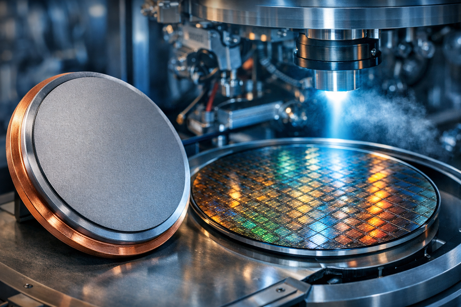
E-Beam evaporation is a physical vapor deposition (PVD) process that uses high-energy electrons to transform solid material into vapor. This vapor subsequently condenses onto a substrate to form a thin, uniform layer. The high-vacuum environment in which this process occurs ensures superior film purity and minimizes contamination. Its ability to deposit films of exceptional quality, even from materials with extremely high melting points, has made it indispensable in many industrial and scientific applications.
The Working Principles of E-Beam Evaporation
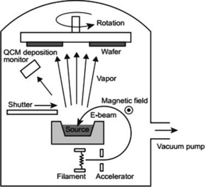
At its core, E-Beam evaporation relies on an electron gun to generate a focused beam of high-energy electrons. These electrons are accelerated to high velocities using a power supply, and their path is carefully controlled by electromagnetic fields. The beam is directed onto a material source placed in a crucible or a water-cooled hearth within a vacuum chamber.
When the electron beam strikes the material source, the intense energy transfer causes localized heating, leading to evaporation of the material. Unlike conventional heating methods, this focused energy minimizes heat dispersion, reducing the risk of damaging temperature-sensitive components nearby. As the material evaporates, its atoms disperse into the vacuum and travel toward the substrate. Upon contact with the substrate’s surface, these atoms condense to form a thin film.
This deposition occurs in a controlled high-vacuum environment, often reaching pressures as low as 10−610^{-6}10−6 to 10−810^{-8}10−8 Torr. Such a vacuum ensures the free path of the vaporized atoms is not hindered by air molecules, resulting in uniform deposition and high film purity.
Advantages of E-Beam Evaporation
One of the most significant benefits of E-Beam evaporation is its ability to handle materials with high melting points. This capability stems from the electron beam’s intense energy, which can vaporize refractory materials like tungsten, molybdenum, and certain ceramics. Additionally, the high-vacuum environment minimizes impurities, ensuring the resulting films are of exceptional purity and consistency.
Another advantage is the level of control it provides over the deposition process. Operators can adjust parameters such as beam intensity and deposition rate to achieve specific film properties. This level of precision is particularly valuable in applications requiring exact thickness or material characteristics, such as optical coatings or semiconductor devices.
However, these benefits come with challenges. The initial cost of E-Beam systems is high due to the complexity of the equipment. Moreover, the process requires skilled operators and regular maintenance to ensure optimal performance. Substrate heating caused by stray electrons can also pose issues for heat-sensitive applications, although innovations such as cryogenic cooling are helping to mitigate these effects.
How Does an E-Beam Evaporator Work?
An E-beam evaporator operates by directing a focused high-energy electron beam onto a material source in a vacuum chamber. This process efficiently vaporizes the material, enabling the deposition of a thin film onto a substrate. Here are additional details about the working principles:
Energy Transfer Through Electron Collisions: The electron beam generated by the electron gun transfers kinetic energy to the material source through high-speed collisions. This localized energy input causes the material to rapidly heat up and vaporize, even for substances with very high melting points.
Substrate Positioning and Uniform Coating: Substrates are often mounted on a rotating stage within the vacuum chamber to ensure even exposure to the vaporized material. This controlled rotation allows for a uniform thin film deposition, which is critical for applications requiring consistent optical or electrical properties across the surface.
What is the Difference Between Sputtering and E-Beam Evaporation?
Sputtering and E-beam evaporation are both popular physical vapor deposition (PVD) techniques, but they differ in their mechanisms, applications, and advantages:
Deposition Mechanism:
1. E-Beam Evaporation uses a high-energy electron beam to heat and vaporize the material directly. The vaporized atoms then condense on the substrate to form a thin film.
2. Sputtering, on the other hand, involves bombarding a target material with high-energy ions (usually from a plasma). The impact dislodges atoms from the target, which then deposit onto the substrate.
Film Adhesion and Uniformity:
1. Sputtering tends to produce films with better adhesion and uniform thickness, even on complex or uneven surfaces, due to the directional energy of the ions and their scattering effects.
2. E-Beam Evaporation, while capable of producing high-purity films, can struggle with uniformity on substrates with intricate geometries.
Deposition Rate:
1. E-Beam Evaporation offers faster deposition rates, making it more suitable for applications where high throughput is required.
2. Sputtering typically has a slower deposition rate but allows for better control of film composition, especially in reactive sputtering processes.
Material Flexibility:
1. E-Beam Evaporation excels in working with high-melting-point materials like refractory metals and ceramics.
2. Sputtering is often preferred for alloy and compound films, as it can easily mix different elements during the deposition process.
These differences make E-beam evaporation and sputtering complementary techniques, each suitable for specific applications depending on the desired film characteristics and material requirements.
Applications of E-Beam Evaporation
E-Beam evaporation is utilized in a broad range of industries and scientific fields, owing to its ability to deposit high-quality films with excellent control over material properties. In the semiconductor industry, it is instrumental in producing thin layers of metals, dielectrics, and semiconductors for devices like transistors and integrated circuits. These films are critical to the functionality and efficiency of modern electronics.
The optics industry relies heavily on this technique to create coatings with specific reflective, refractive, or absorptive properties. For instance, anti-reflective coatings on lenses and mirrors used in lasers and cameras are typically produced through E-Beam evaporation. Similarly, the method is used to fabricate high-reflectivity mirrors and beam splitters for advanced optical systems.
In the field of renewable energy, E-Beam evaporation contributes to the efficiency of solar panels by depositing conductive and anti-reflective coatings. These layers improve light absorption and reduce energy loss, enhancing the overall performance of photovoltaic cells. Aerospace and defense applications also benefit from the durability and precision of thin films deposited through this method, which are used in sensors, protective coatings, and optical devices.
Technological Innovations and Advancements
Recent advancements in E-Beam evaporation technology have expanded its capabilities and improved its efficiency. Automation has played a significant role, with modern systems integrating advanced control and monitoring tools to ensure consistent film quality. Real-time feedback mechanisms, such as quartz crystal microbalances and spectroscopic ellipsometry, enable precise control of film thickness and optical properties during deposition.
Multi-source configurations represent another significant innovation. These systems allow the simultaneous evaporation of different materials, making it possible to create complex multi-layered films with unique properties. This is particularly useful in the production of dielectric mirrors or advanced optical coatings.
Cryogenic cooling is a notable enhancement that addresses the issue of substrate heating. By maintaining a low substrate temperature, this innovation expands the range of materials and applications suitable for E-Beam evaporation, particularly for temperature-sensitive substrates.
Comparison with Other Deposition Techniques
Compared to thermal evaporation, E-Beam evaporation offers superior control and versatility. Thermal evaporation, which relies on resistive heating, struggles to handle high-melting-point materials and often results in less precise deposition. Sputtering, another common PVD technique, excels in producing films with strong adhesion and high uniformity, but its lower deposition rates and more complex process make it less suitable for applications requiring rapid and large-scale deposition.
E-Beam evaporation’s unique combination of high precision, material flexibility, and film purity distinguishes it as a preferred method for demanding applications. However, the choice of deposition technique ultimately depends on the specific requirements of the application, including material properties, film characteristics, and cost considerations.
The Future of E-Beam Evaporation
As materials science and technology continue to advance, the demand for thin films with novel properties will only grow. E-Beam evaporation is poised to meet these challenges, with ongoing research focused on enhancing its capabilities and expanding its applications. The development of nanostructured films, for instance, is opening new avenues in areas like plasmonics, quantum computing, and bioengineering. These films require the precise control and high purity that E-Beam evaporation provides.
Efforts to make the process more sustainable are also gaining momentum. Innovations aimed at reducing energy consumption and optimizing material usage are making E-Beam evaporation more environmentally friendly. Hybrid techniques that combine E-Beam evaporation with other deposition methods, such as atomic layer deposition (ALD), are being explored to achieve even greater precision and functionality.
The integration of advanced materials, including two-dimensional materials like graphene and exotic alloys, is further expanding the possibilities for E-Beam evaporation. As these innovations continue to emerge, the technique is set to remain a cornerstone of thin film deposition for years to come.
Conclusion
E-Beam evaporation is a powerful and versatile tool for thin film deposition, offering unmatched precision, purity, and flexibility. Its ability to work with a wide range of materials and its applications across industries highlight its importance in modern technology. Despite its challenges, continuous advancements are making it more efficient and accessible, ensuring its relevance in an increasingly complex and demanding technological landscape. Understanding E-Beam evaporation and its potential is essential for researchers and engineers striving to push the boundaries of materials science and device fabrication.