Introduction
Beryllium (Be) Sputtering Targets are high-performance metallic targets used in thin film deposition processes for specialized electronic, optical, and aerospace applications. Beryllium is a lightweight metal with exceptional stiffness, high thermal conductivity, and excellent transparency to X-rays, making it a unique material for advanced thin film technologies.
In Physical Vapor Deposition (PVD) processes such as DC magnetron sputtering, beryllium sputtering targets enable the deposition of ultra-thin Be films with excellent mechanical stability and thermal performance. These thin films are particularly valuable in high-precision instruments, semiconductor devices, and scientific equipment where lightweight materials with exceptional thermal and mechanical properties are required.
Detailed Description
Beryllium Sputtering Targets are manufactured from high-purity beryllium metal using powder metallurgy and advanced consolidation techniques such as hot pressing or hot isostatic pressing (HIP). These methods produce dense, homogeneous targets with stable microstructure and reliable sputtering behavior.
Beryllium has several distinctive material characteristics that make it useful for thin film applications:
Extremely low density (1.85 g/cm³)
High stiffness-to-weight ratio
Excellent thermal conductivity
Low X-ray absorption
High dimensional stability
These properties allow beryllium thin films to function effectively in precision optical systems, aerospace instruments, and semiconductor devices.
Due to its electrical conductivity, beryllium targets are typically used in DC magnetron sputtering systems, which allow efficient deposition rates and uniform thin film formation. Beryllium thin films can be used as structural coatings, protective layers, or functional metallic films depending on the application.
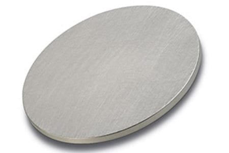
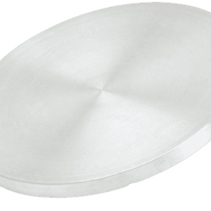
Beryllium sputtering targets are available in various shapes including circular discs, rectangular plates, and custom geometries to fit different sputtering cathodes. For large-area deposition systems or high-power sputtering processes, the targets can be bonded to copper backing plates using indium bonding or elastomer bonding to improve thermal dissipation and mechanical stability.
Because beryllium dust can be hazardous during machining and processing, manufacturing and handling of these targets require strict environmental and safety controls to ensure safe production and usage.
Applications
Thin films deposited from Beryllium Sputtering Targets are used in a variety of advanced technological fields:
X-ray optics and detectors – beryllium coatings used in X-ray transmission windows and detector components.
Semiconductor manufacturing – thin films used in specialized electronic components and device research.
Aerospace and scientific instruments – lightweight metallic coatings used in precision equipment.
Optical systems – coatings for mirrors and optical components requiring high stiffness and thermal stability.
Protective coatings – thin films with high durability and dimensional stability.
Materials science research – experimental thin films for advanced structural materials.
Technical Parameters
| Parameter | Typical Value / Range | Importance |
|---|---|---|
| Purity | 99.0% – 99.9% | High purity improves film quality and device performance |
| Density | ≥98% theoretical | Ensures stable sputtering and uniform deposition |
| Diameter | 25 – 300 mm (custom) | Compatible with various sputtering systems |
| Thickness | 3 – 6 mm | Influences sputtering rate and target lifetime |
| Bonding | Copper backing plate (optional) | Improves heat dissipation and structural stability |
Comparison with Related Materials
| Material | Key Advantage | Typical Application |
|---|---|---|
| Beryllium (Be) | Extremely lightweight with high stiffness | Aerospace and precision optical systems |
| Aluminum (Al) | Good conductivity and low cost | General thin film coatings |
| Titanium (Ti) | Excellent adhesion and corrosion resistance | Protective and structural coatings |
FAQ
| Question | Answer |
|---|---|
| Can beryllium sputtering targets be customized? | Yes, diameter, thickness, purity, and backing plate bonding options can be customized according to sputtering system requirements. |
| Which sputtering method is recommended for beryllium targets? | DC magnetron sputtering is typically used because beryllium is electrically conductive. |
| Are bonded targets available? | Yes, beryllium targets can be indium-bonded or elastomer-bonded to copper backing plates for improved heat dissipation. |
| What substrates are compatible with beryllium thin films? | Silicon wafers, glass, ceramics, and metal substrates are commonly used depending on the application. |
| Which industries commonly use beryllium sputtering targets? | Aerospace, semiconductor research, X-ray optics manufacturing, and scientific instrumentation industries. |
Packaging
Our Beryllium Sputtering Targets are meticulously tagged and labeled externally to ensure efficient identification and maintain strict quality control standards. Each target is vacuum-sealed and packaged with protective materials to prevent contamination or damage during storage and transportation. Export-grade cartons or wooden crates are used to ensure safe delivery.
Conclusion
Beryllium Sputtering Targets provide a unique combination of lightweight structure, high stiffness, excellent thermal conductivity, and X-ray transparency, making them ideal for specialized thin film applications in aerospace, semiconductor research, and scientific instrumentation.
With high purity levels, customizable dimensions, and reliable manufacturing processes, beryllium sputtering targets offer consistent performance for advanced thin film deposition systems.
For detailed specifications and a quotation, please contact us at sales@thinfilmmaterials.com.


Reviews
There are no reviews yet.