Introduction
Diamond, long revered as the hardest natural material, has transcended its traditional associations with gemstones and luxury. In modern science and technology, synthetic diamond thin films have emerged as one of the most promising materials for next-generation electronic, optical, and quantum devices. A recent research collaboration between Peking University Dongguan Optoelectronic Research Institute and the Southern University of Science and Technology has resulted in a revolutionary breakthrough: the successful synthesis of large-area, ultra-smooth, and ultra-flexible diamond thin films. This innovation, published in Nature, paves the way for industrial-scale applications and could redefine multiple high-tech sectors.
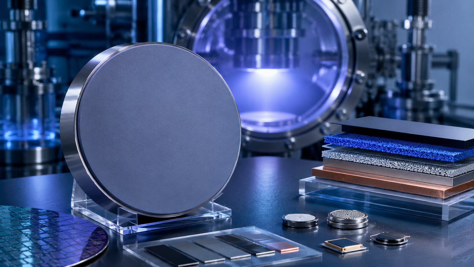
TFM (Thin Film Materials), a global supplier of advanced sputtering targets and deposition materials, is poised to play a key role in supporting this revolution. By providing high-purity materials, tailored substrates, and precision-engineered bonding solutions, TFM empowers researchers and manufacturers to integrate these cutting-edge diamond films into their products and systems.
Scientific and Technical Background
The Challenge of Scaling Diamond Thin Films
Traditional methods for producing synthetic diamond films using chemical vapor deposition (CVD) have been limited by scalability, surface roughness, and structural imperfections. Conventional CVD-grown diamond films were often brittle, uneven, or difficult to integrate into flexible electronics. These limitations hindered their widespread adoption in commercial settings.
The new approach combines advanced CVD techniques with nanostructured seed layers and gas-phase composition control to yield a single-crystal diamond film with:
- Ultra-low surface roughness (<1 nm RMS)
- Mechanical flexibility without compromising thermal conductivity
- Wafer-scale uniformity (up to several inches)
- Superior optical transparency and electrical insulation
These properties make the new diamond films ideal for a wide range of applications, including those in extreme environments, quantum technology, and optoelectronics.
Material Properties of Diamond Thin Films
Diamond’s unique combination of mechanical, thermal, optical, and electrical characteristics has made it highly desirable in many high-tech industries:
- Hardness: 10 on the Mohs scale; excellent for wear-resistant coatings
- Thermal Conductivity: ~2000 W/m·K, the highest of any bulk material
- Bandgap: ~5.5 eV, suitable for high-power electronic and photonic devices
- Optical Transparency: Transmits from deep ultraviolet to infrared
- Dielectric Strength: High resistance to electrical breakdown
These attributes allow diamond films to function under conditions that would degrade or destroy other materials.
Applications Enabled by the Breakthrough
1. Quantum Computing and Photonics
Synthetic diamond films with engineered nitrogen-vacancy (NV) centers enable advanced quantum technologies. These defects act as stable quantum bits (qubits) for sensing, imaging, and computation. The ultra-smooth and low-strain diamond films produced by this new method improve coherence times and photon emission stability.
TFM supports this market by providing:
- High-purity Carbon Sputtering Targets for controlled doping
- Niobium and Tantalum Sputtering Targets for qubit control circuitry
- Substrate Backing Plates and Carriers for precise alignment and heat management
2. Flexible and Wearable Electronics
The development of foldable and wearable devices demands materials that combine flexibility with mechanical resilience. Diamond thin films deliver an unprecedented combination of flexibility, thermal management, and scratch resistance.
TFM enables integration by supplying:
- Flexible Substrate Films (e.g., Polyimide, PEN) for roll-to-roll processing
- Silicon Carbide and Boron Nitride Targets for intermediate or buffer layers
- Customized Diamond-Like Carbon (DLC) Coating Targets
3. High-Frequency Power Electronics
Wide-bandgap semiconductors like GaN and SiC have transformed the landscape of power electronics. However, managing heat in such systems remains a bottleneck. Diamond films, with their high thermal conductivity, provide ideal heat spreaders and dielectric barriers.
TFM contributes to this space through:
- Molybdenum, Tungsten, and Titanium Sputtering Targets for thermal interface layers
- Advanced Target Bonding Services to integrate diamond films with heat sinks or packages
- Electrically Conductive Adhesives and Backing Alloys
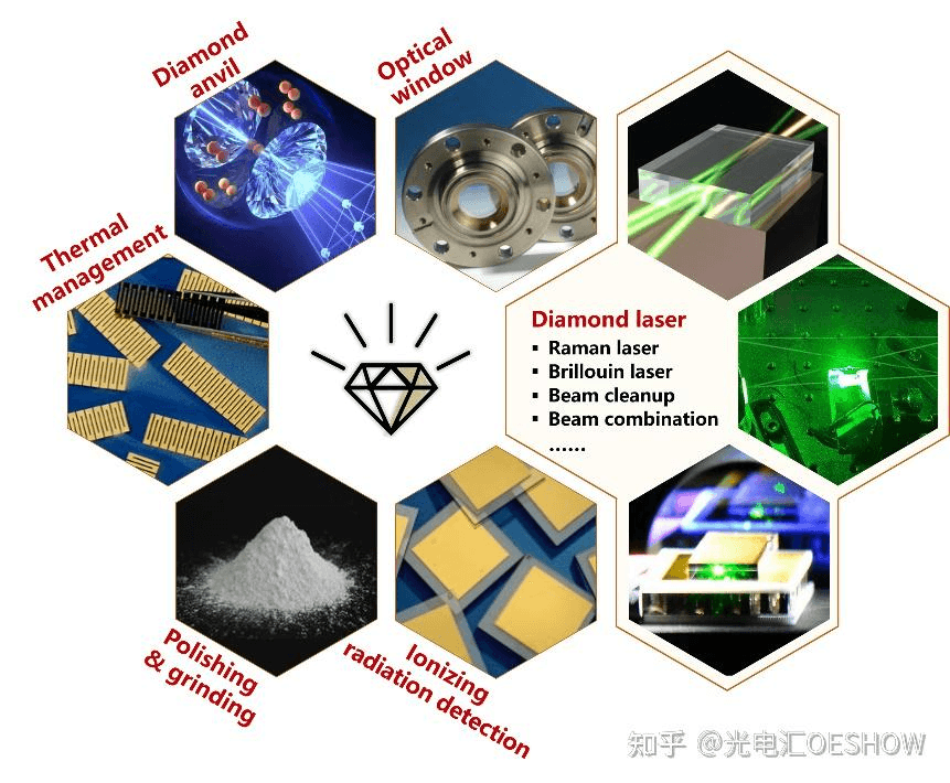
4. Optical and Infrared Applications
Diamond’s wide transmission window and low absorption make it an excellent material for high-power lasers, IR optics, and transparent windows in extreme environments.
TFM supplies complementary materials including:
- Germanium and Zinc Selenide Sputtering Targets for IR optics
- Aluminum Nitride and Magnesium Fluoride Coatings
- Diamond-Compatible Mounting Systems for high-temperature operation
5. Biomedical Devices
Biocompatible and chemically inert, diamond films have applications in implantable sensors, biosensors, and diagnostic devices. The ability to produce flexible, wafer-scale diamond films expands their usability in medical technology.
TFM supports this by offering:
- Biocompatible Metal Targets (e.g., Titanium, Platinum)
- Micropatterned Substrates and Masks
- Ultra-clean Packaging and Surface Preparation Services
Integration with TFM’s Material Solutions
TFM’s extensive product line is designed to meet the rigorous demands of advanced thin film fabrication. Diamond film development teams can rely on TFM for the following integrated solutions:
| TFM Product | Function | Form |
|---|---|---|
| Carbon Targets | Precursor or dopant source | Disc, Planar |
| SiC, BN Targets | Buffer/insulating layers | Planar, Cylindrical |
| High-Purity Metals | Electrodes, interconnects | Sheet, Rod, Plate |
| Flexible Substrates | Roll-to-roll base films | Roll, Sheet |
| Bonding Services | Film-to-substrate joining | Elastomeric, Indium alloy |
| Custom Engineering | Full-stack material design | Project-based |
TFM’s research-grade purity (up to 99.9995%) ensures that customers can achieve reliable film growth with consistent electrical, mechanical, and optical performance.
Market Dynamics and Strategic Opportunities
Current Trends
- Miniaturization: Drives demand for thinner, more functional films.
- Thermal Management: Emerging 3D ICs and power modules require advanced heat dissipation.
- Quantum Sensing and Computing: Rapid investment in scalable quantum technologies.
- Green Electronics: Sustainable and long-lasting materials are in high demand.
Market Projections
Analysts project the global synthetic diamond market to exceed USD 30 billion by 2030, with diamond films contributing significantly to this value. Key growth sectors include:
- Consumer electronics (foldable phones, AR/VR)
- Aerospace and defense (radiation-resistant optics)
- Industrial machinery (wear coatings)
- Medical diagnostics (biosensing platforms)
TFM’s strong international supply chain and customer support infrastructure make it a preferred partner for institutions and enterprises navigating this growth.
Case Study: From Lab to Production
A leading photonics company recently collaborated with TFM to integrate synthetic diamond films into next-gen IR windows. Challenges included thermal mismatch, delamination, and sputtering uniformity. By leveraging TFM’s:
- Customized Molybdenum bonding base
- In-house bonding of diamond films with controlled heating cycles
- Surface activation prior to DLC coating
The company achieved a 30% improvement in thermal cycling reliability and a 25% increase in infrared transmittance across the 3–8 µm band. This successful scale-up demonstrates how TFM supports both innovation and commercialization.
Conclusion: Empowering the Diamond Film Revolution
The development of ultra-smooth, large-area, and flexible diamond thin films marks a turning point in materials science. With unparalleled thermal, mechanical, and optical performance, these films are set to reshape industries ranging from quantum electronics to wearable technology.
TFM is committed to supporting this shift through:
- A complete portfolio of compatible sputtering targets
- High-purity materials for precision deposition
- Engineering support for full-stack integration
- Custom bonding and substrate services
As the demand for robust, high-performance materials accelerates, TFM remains a trusted partner for research institutions and commercial manufacturers alike. Whether you are developing quantum chips or rugged optical coatings, TFM provides the materials and expertise to help you innovate with confidence.