Introduction: A New Era of Thin Film Manufacturing
The thin film industry has long stood at the intersection of innovation and precision. Whether in semiconductors, solar cells, optical coatings, or advanced sensors, thin film deposition plays a vital role in modern technologies. However, optimizing thin film processes has traditionally been a laborious task involving trial-and-error, extensive physical modeling, and a deep understanding of material science. In recent years, Artificial Intelligence (AI) and Machine Learning (ML) have emerged as transformative forces in this landscape, offering unprecedented tools for accelerating discovery, reducing costs, and improving performance.
As industries continue to pursue green energy, high-speed electronics, and quantum computing, integrating AI and ML into thin film process optimization isn’t just a competitive advantage—it’s becoming a necessity. This article explores how these advanced technologies are reshaping thin film processes and helping manufacturers achieve smarter, faster, and more sustainable production.
The Challenges of Thin Film Process Optimization
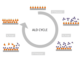
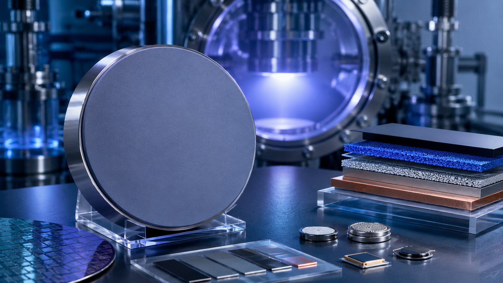
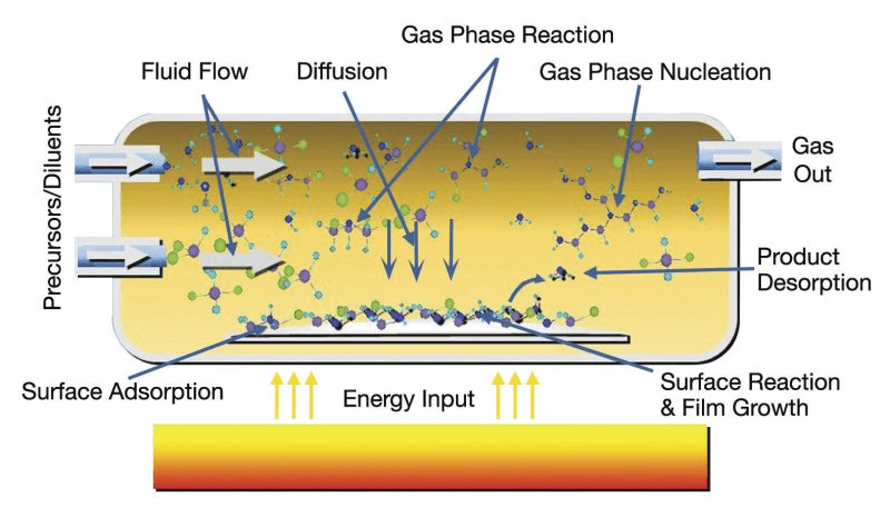
Thin film deposition techniques—such as sputtering, chemical vapor deposition (CVD), atomic layer deposition (ALD), and electron-beam evaporation—each present a complex interplay of variables. Parameters like substrate temperature, deposition rate, gas flow, and plasma power must be carefully balanced to achieve the desired film thickness, uniformity, adhesion, and material phase.
Historically, this balance has been achieved through extensive design of experiments (DoE) and physical modeling, which are both time-consuming and costly. Additionally, these methods often struggle to capture nonlinear relationships and hidden correlations among parameters.
Limitations of Traditional Approaches:
- Time-intensive process development
- High material and labor costs
- Inflexibility in dynamic manufacturing environments
- Inability to scale across different materials or substrates
- Difficulty in interpreting complex, multidimensional data
Enter machine learning algorithms, which excel at extracting patterns from large datasets and making predictions based on them.
How AI and Machine Learning Are Revolutionizing Thin Film Technology
1. Predictive Modeling of Thin Film Properties
One of the most promising applications of machine learning in thin film technology is the development of predictive models for film characteristics such as thickness, refractive index, roughness, and electrical conductivity.
By training ML algorithms on historical process data, manufacturers can build models that predict the outcome of a deposition run before it happens. This allows for real-time adjustments and prevents wasteful trial-and-error experiments.
Popular techniques include:
- Regression models (e.g., linear regression, support vector regression)
- Neural networks (e.g., deep learning for complex patterns)
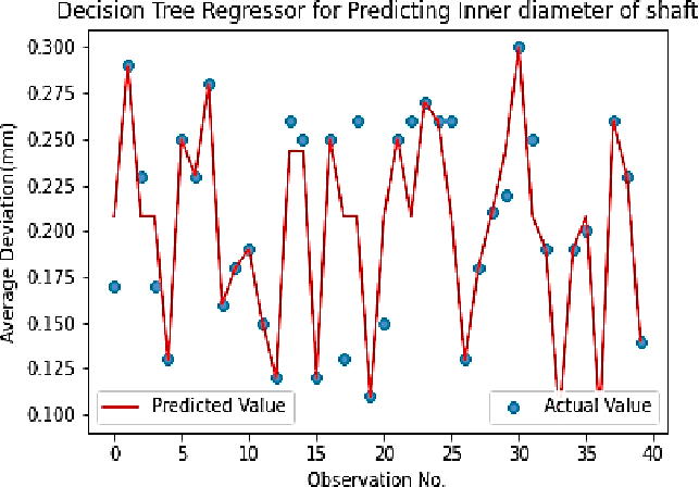
- Decision trees and ensemble methods (e.g., random forests)
These models can optimize both process parameters and equipment settings, significantly shortening development time for new materials or layer stacks.
2. Real-Time Process Control and Feedback
In dynamic thin film deposition environments, conditions can change rapidly due to variations in pressure, power, and target erosion. AI-powered systems can implement closed-loop control, adjusting process parameters on-the-fly based on sensor feedback and model predictions.
For example, in magnetron sputtering, fluctuations in plasma density or target condition can result in non-uniform coatings. AI systems monitor these fluctuations in real time and adjust parameters such as power input or gas flow, maintaining consistent film properties across the entire wafer.
This adaptive process control has been deployed in:
- In-line metrology systems
- AI-driven plasma diagnostics
- Smart vacuum control systems
- Optical emission spectroscopy (OES) with ML enhancements
3. Defect Detection and Classification
Surface defects, pinholes, and particulate contamination in thin films can drastically reduce product yields. Traditional inspection methods rely on manual inspection or basic imaging, both of which are limited in speed and accuracy.
Using computer vision and deep learning, AI systems can now detect, classify, and even localize defects in real-time, enabling immediate correction or classification of out-of-spec products.
AI-based image analysis tools are commonly used for:
- SEM image classification
- AFM data interpretation
- Inline optical inspection
- Early detection of plasma instabilities
By integrating these tools into process monitoring systems, manufacturers can automatically reject defective wafers or trigger process recalibration.
Case Studies: AI in Action in Thin Film Industries
Case Study 1: Semiconductor Fabrication
In advanced semiconductor nodes (e.g., 5nm and below), layer uniformity and defect control are critical. A leading chipmaker integrated a machine learning framework using Bayesian optimization to tune ALD parameters for high-k dielectric layers.
Results:
- 30% reduction in process development time
- Improved film conformality and uniformity
- Reduced precursor consumption
Case Study 2: Solar Panel Manufacturing
Thin film photovoltaic manufacturers (CdTe, CIGS) have employed convolutional neural networks (CNNs) for real-time defect detection in transparent conductive oxide (TCO) layers. The AI system improved detection accuracy by 40% and reduced the false positive rate.
Case Study 3: Optical Coating for Lenses
A major optics company implemented AI to optimize multilayer antireflection coatings, using a genetic algorithm combined with a neural network. The model predicted optimal refractive index profiles to achieve near-zero reflectance over a wide wavelength range.
Key AI and ML Techniques in Thin Film Optimization
1. Supervised Learning
Trains algorithms on labeled datasets. Common in:
- Property prediction (thickness, conductivity)
- Recipe classification
- Defect labeling
2. Unsupervised Learning
Finds patterns in unlabeled data. Useful for:
- Clustering similar process runs
- Detecting anomalies
- Data compression and dimensionality reduction
3. Reinforcement Learning
Uses reward-based learning to optimize control strategies in real-time. Promising in:
- Dynamic plasma control
- Substrate movement in spatial ALD
- Adaptive power modulation
4. Deep Learning
Capable of handling high-dimensional, unstructured data like images, time-series, and sensor arrays.
Applications include:
- Spectral data interpretation
- Plasma diagnostics
- Predicting process drift
The Role of Big Data and IoT in AI-Driven Thin Film Manufacturing
Data is the Fuel
AI cannot function without large, clean, and contextualized datasets. Thin film systems are increasingly equipped with Internet of Things (IoT) sensors that generate real-time data streams from pressure gauges, temperature sensors, deposition monitors, and spectrometers.
Using data lakes and cloud platforms, manufacturers can collect and analyze petabytes of data, enabling cross-site process optimization and global recipe standardization.
Google Cloud, AWS, and Microsoft Azure are already offering AI-as-a-Service platforms tailored for manufacturing environments, including support for edge computing to reduce latency.
Challenges and Limitations of AI in Thin Film Processes
While the potential is vast, integrating AI into thin film manufacturing is not without its challenges:
- Data Quality and Volume: Many legacy systems were not designed with data science in mind.
- Model Interpretability: AI models, especially deep learning ones, often function as black boxes.
- Domain Expertise: AI needs to be guided by domain-specific knowledge to avoid spurious correlations.
- Integration Costs: Retrofitting existing equipment with sensors and AI systems can be expensive.
- Security and IP Concerns: Cloud-based solutions must comply with stringent data security policies.
Despite these challenges, the trend toward smart manufacturing is irreversible, and companies that embrace AI stand to gain a significant edge.
Future Directions: Where AI in Thin Film Optimization is Headed
1. Digital Twins
By creating virtual replicas of deposition systems, AI can simulate thousands of process conditions in silico, greatly accelerating R&D.
2. Self-Optimizing Chambers
Imagine a deposition tool that tunes itself based on AI recommendations. These “self-driving” chambers are being developed, with early prototypes already showing promise in adjusting power, pressure, and gas flows autonomously.
3. AI-Guided Material Discovery
AI isn’t just optimizing processes—it’s also discovering new materials. Generative models and active learning strategies are helping scientists predict the properties of unexplored thin film compounds.
4. Democratization of Thin Film Design
With platforms offering AI-based simulation and recipe prediction, even small labs or startups can now access capabilities previously limited to major fabs.
Conclusion: Intelligence is the New Precision
As the thin film industry becomes increasingly complex and competitive, embracing AI and machine learning is no longer optional—it is essential. These technologies promise faster process optimization, improved yield, real-time quality control, and even the discovery of new materials.
Companies that invest early in AI infrastructure, talent, and data strategy will not only reduce costs and enhance performance but also lead the next wave of smart materials engineering.
In the rapidly evolving world of advanced materials and nanotechnology, AI is not just a tool—it is a strategic differentiator.
Frequently Asked Questions
What is the role of AI in thin film deposition?
AI helps predict film properties, control deposition parameters in real-time, detect defects, and discover optimal recipes for new materials—all by analyzing large datasets and learning from historical outcomes.
Can AI reduce the cost of thin film manufacturing?
Yes. By minimizing trial-and-error, optimizing material use, and preventing defects, AI significantly cuts both operational and material costs.
Which machine learning algorithms are used in thin film processing?
Common algorithms include regression models, neural networks, support vector machines, decision trees, and reinforcement learning frameworks.
Is AI used in solar thin film production?
Absolutely. AI is widely used in CIGS and CdTe solar panel production for process control, defect detection, and efficiency optimization.