Generic selectors
Exact matches only
Search in title
Search in content
Post Type Selectors

Nickel Antimony Telluride(Ni₂SbTe₂) Target

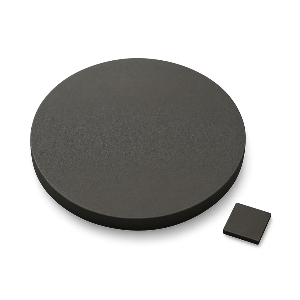
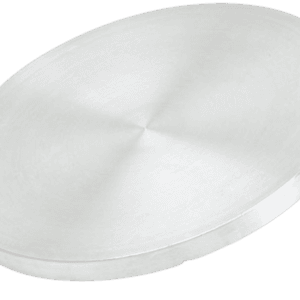
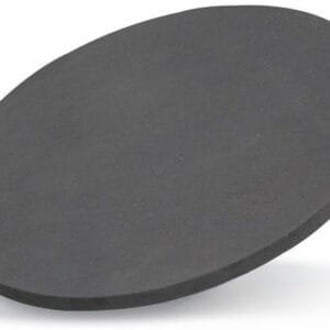
Nickel Antimony Telluride (Ni₂SbTe₂) Sputtering Target is a compound material widely used in the fabrication of thin films for electronic and thermoelectric applications. This ternary chalcogenide combines the properties of nickel, antimony, and tellurium, offering a unique blend of electrical conductivity and thermal stability. Ni₂SbTe₂ targets are particularly valued in research and development of phase-change memory devices, topological insulators, and next-generation thermoelectric materials.

Manufactured with high purity and precise stoichiometry, Ni₂SbTe₂ targets are typically available in disk or rectangular forms, with optional bonding to copper backing plates for enhanced thermal management during deposition. These targets are compatible with various physical vapor deposition (PVD) techniques, such as magnetron sputtering, enabling uniform film growth on semiconductor and oxide substrates.

Due to its tunable band structure and promising electronic characteristics, Nickel Antimony Telluride continues to gain attention in advanced materials research and nanoelectronics.

Reviews

There are no reviews yet.

Be the first to review “Nickel Antimony Telluride(Ni₂SbTe₂) Target”

Your email address will not be published. Required fields are marked *

Related Products

FAQ

It’s the source material (in solid form) used in sputter deposition to eject atoms or molecules that then form a thin film on a substrate.

Targets can be pure metals (e.g., gold, copper, aluminum), ceramics (e.g., Al₂O₃, SiO₂, TiO₂), alloys, or composites—chosen based on the film’s desired properties.


They are produced by processes such as melting/casting for metals or sintering (often with hot isostatic pressing) for ceramics and composite targets to ensure high density and purity.


In a vacuum chamber, a plasma (typically argon) bombards the target, ejecting atoms that travel and condense on a substrate, forming a thin film.


Key factors include the target’s purity, density, grain structure, and the sputtering yield (i.e. how many atoms are ejected per incident ion), as well as operating conditions like power density and gas pressure.


Operators monitor target erosion (often by measuring the depth of the eroded “race track”) or track total energy delivered (kilowatt-hours) until it reaches a threshold that can compromise film quality.


Fragile materials (such as many ceramics or certain oxides) and precious metals often require a backing plate to improve cooling, mechanical stability, and to allow thinner targets that reduce material costs.


DC sputtering is used for conductive targets, while RF sputtering is necessary for insulating targets (like many oxides) because it prevents charge buildup on the target’s surface.


In reactive sputtering, a reactive gas (e.g., oxygen or nitrogen) is introduced to form compound films on the substrate, but it may also “poison” the target surface if not carefully controlled.


Many manufacturers prefer to control raw material quality by sourcing their own powders; using external powders can risk impurities and inconsistent target properties.


Targets should be stored in clean, dry conditions (often in original packaging or re-wrapped in protective materials) and handled with gloves to avoid contamination, ensuring optimal performance during deposition.

Deposition rate depends on factors such as target material and composition, power density, working gas pressure, substrate distance, and the configuration of the sputtering system (e.g., magnetron design).

 
Shopping Cart
Scroll to Top