1. Introduction: The Central Role of EUV Lithography in Semiconductor Scaling
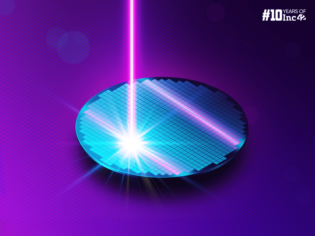
Semiconductor manufacturing has continuously pursued smaller feature sizes, from micrometers down to single nanometers. With Moore’s Law under pressure, the transition to extreme ultraviolet (EUV) lithography has been pivotal for enabling nodes below 7 nm. EUV lithography uses 13.5 nm wavelength light to pattern features previously impossible with deep ultraviolet (DUV) techniques.
At the heart of EUV patterning are photomasks—complex multilayered optical components that reflect EUV light with extreme precision. These masks are constructed from stacks of molybdenum and silicon, capped and protected with additional materials, and patterned with absorber layers that define circuit features.
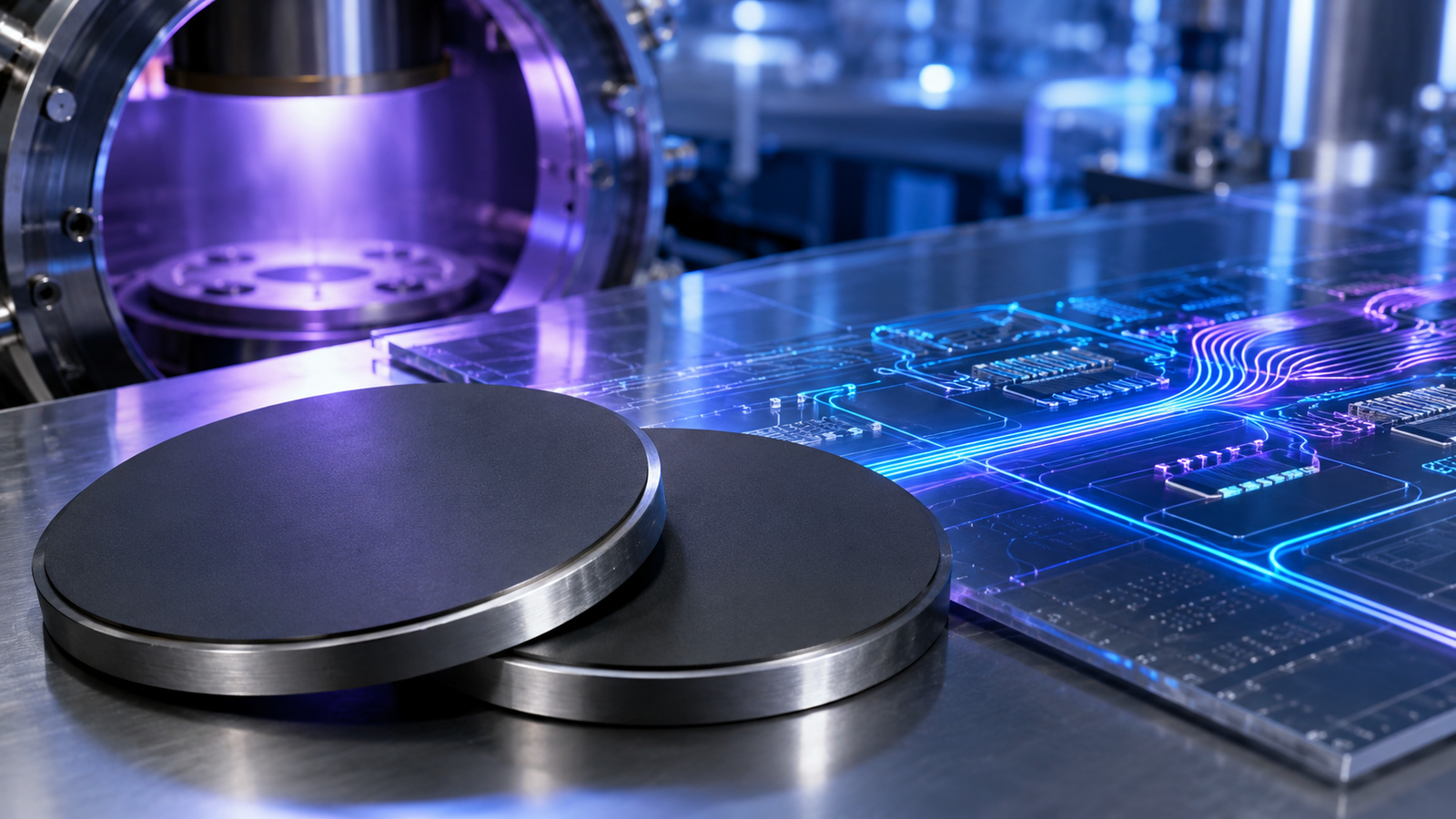
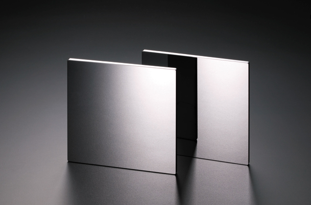
To fabricate these masks, sputtering targets are essential. Materials such as Mo, Si, Ru, Ta-based compounds, and absorbers like TaBN or TaN are deposited via sputtering to form highly controlled films. Without precision-engineered sputtering targets, the consistency, reflectivity, and defect tolerance of EUV masks would not meet industrial standards.
This article explores the science and engineering of sputtering targets for EUV lithography masks, focusing on materials, challenges, and innovations that enable the next generation of semiconductor manufacturing.
2. Fundamentals of EUV Lithography Masks
2.1 The EUV Reflective Mask Structure
Unlike DUV masks that transmit light through quartz substrates, EUV masks rely on multilayer Bragg reflectors:
- Substrate: Ultra-flat, defect-free glass or low-thermal-expansion material (LTEM).
- Multilayer Stack: ~40 alternating layers of Mo and Si, each ~7 nm thick, forming a mirror with ~70% reflectivity at 13.5 nm.
- Capping Layer: Ru or similar materials for surface protection and reflectivity tuning.
- Absorber Layer: TaBN, TaN, or MoSi-based compounds that define the pattern.
- Anti-reflective / buffer layers: Improve pattern fidelity.
2.2 Film Quality Requirements
- Interface roughness <0.2 nm across 40 bilayers.
- Uniform thickness control at the angstrom scale.
- Ultra-low defect density, since a single particle can ruin a mask worth >$100,000.
These extreme requirements mean that sputtering targets must be manufactured to unmatched standards of purity and homogeneity.
3. Critical Sputtering Target Materials for EUV Masks
3.1 Molybdenum (Mo) Targets
- Role: Primary reflective layer in multilayers.
- Requirements: 99.999% purity, extremely fine grain size, minimal oxygen contamination.
- Challenges: Oxygen or carbon impurities create interfacial roughness and reduce reflectivity.
3.2 Silicon (Si) Targets
- Role: Alternating layer with Mo in the Bragg stack.
- Requirements: High-density polycrystalline Si, with oxygen levels <10 ppm.
- Challenges: Avoiding particulate formation during sputtering.
3.3 Ruthenium (Ru) Targets
- Role: Capping layer, improves oxidation resistance and reflectivity.
- Challenges: Expensive material, high sputtering cost, needs high density to prevent spitting.
3.4 Tantalum-Based Absorber Targets (TaBN, TaN, TaSiN)
- Role: Define absorber features to block EUV light where needed.
- Requirements: Amorphous film growth, high etch selectivity, low stress.
- Challenges: Precise stoichiometry in Ta–B–N films to maintain uniform absorption at 13.5 nm.
3.5 Buffer and Anti-Reflective Targets
- Materials like Cr, Ti, or Al-based compounds may be used in underlayers to control stress and reflection.
4. Fabrication of Sputtering Targets for EUV Applications
Producing these targets requires extreme precision:
- Powder Synthesis: Ultra-high purity starting powders (>99.999%).
- Densification: Hot isostatic pressing (HIP) or spark plasma sintering (SPS) to eliminate pores.
- Grain Size Control: Sub-micron grains ensure uniform sputtering.
- Bonding: Targets must be bonded to backing plates (Cu, Al) to handle high sputtering power.
- Defect Elimination: Non-destructive testing for inclusions, cracks, or secondary phases.
For compound targets like TaBN, reactive sintering and dopant control are essential to maintain film stoichiometry.
5. Deposition Techniques and Film Properties
5.1 Magnetron Sputtering
- DC or RF magnetron sputtering is standard for EUV mask materials.
- Requires ultra-clean chambers with base pressures <1 × 10⁻⁷ Torr.
5.2 Multilayer Deposition
- 40+ alternating Mo/Si layers demand sub-angstrom control of deposition rates.
- Any deviation causes cumulative phase errors, reducing EUV reflectivity.
5.3 Absorber Layer Deposition
- Reactive sputtering for TaBN requires precise nitrogen/argon gas flow.
- Uniform composition across 6-inch wafers is mandatory.
6. Challenges in EUV Mask Material Deposition
- Defectivity: Even a single particle can cause catastrophic yield loss.
- Stress Control: Thick absorber layers must avoid cracking or delamination.
- Interdiffusion: Mo and Si intermix at high temperatures, degrading reflectivity. Barrier layers are sometimes added.
- Target Poisoning: In reactive sputtering, excessive nitrogen can alter target surface chemistry, leading to unstable deposition.
7. Innovations and Future Directions
7.1 Improved Target Fabrication
- Nanostructured powders for denser targets.
- Grain boundary engineering to minimize particle ejection.
- Recycling technologies to lower Ru and Ta costs.
7.2 Advanced Materials
- New absorbers such as MoSi, Ru-based compounds, or high-k dielectrics.
- Capping layers with improved oxidation resistance beyond Ru.
7.3 Hybrid Deposition
- Combining sputtering with atomic layer deposition (ALD) for atomic-level interface control.
7.4 EUV Pellicle-Compatible Coatings
- Development of low-stress absorbers that remain stable under pellicle exposure.
8. Conclusion
The success of EUV lithography—and by extension, the continuation of semiconductor scaling—depends on the ability to fabricate defect-free, high-reflectivity, high-stability EUV masks. At the foundation of this effort lie sputtering targets: Mo and Si for multilayers, Ru for capping, and Ta-based absorbers.
The fabrication of these targets demands the highest levels of purity, homogeneity, and structural integrity. Suppliers such as TFM are pushing the boundaries of materials science with advanced sintering, powder synthesis, and bonding technologies to meet the stringent requirements of EUV mask production.
As semiconductor technology marches toward 2 nm and beyond, sputtering targets for EUV masks will remain a critical enabling technology. Future advances will focus on reducing defects, enhancing material stability, and lowering costs, ensuring that EUV lithography continues to drive the semiconductor industry forward.