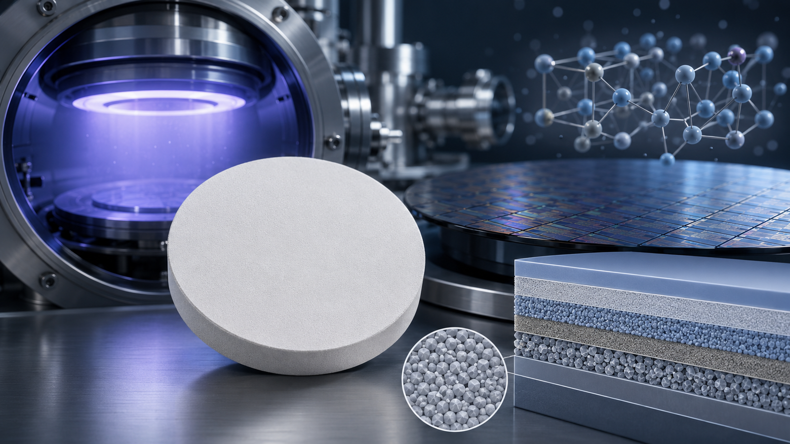
Introduction: The Evolution of Advanced Coating Technologies
The field of surface engineering has undergone a dramatic transformation in recent decades, driven by the demand for high-performance, durable, and functional coatings. Industries spanning from semiconductor manufacturing , aerospace, optics, and energy to medical devices and automotive engineering all rely on precise, reliable coatings to enhance product longevity and functionality. Among the myriad coating technologies, Physical Vapor Deposition (PVD) and Atomic Layer Deposition (ALD) have emerged as two of the most influential processes. Recent developments have fostered the integration of these two methods into hybrid PVD–ALD processes, unlocking unprecedented opportunities for advanced coatings.
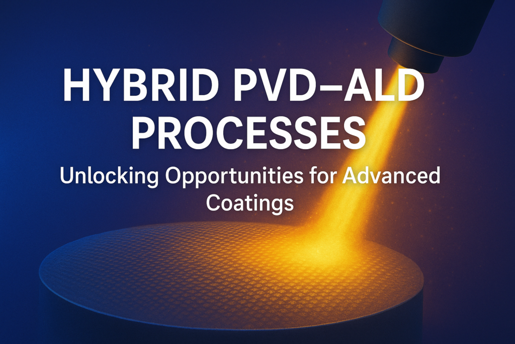
This article provides an in-depth exploration of hybrid PVD–ALD processes, examining their underlying principles, technical advantages, challenges, and transformative impact across various industries. We will also analyze emerging trends, simulation-aided design, digital manufacturing integration, and prospects for next-generation vacuum coating technologies.
Fundamentals of PVD and ALD
Physical Vapor Deposition (PVD)
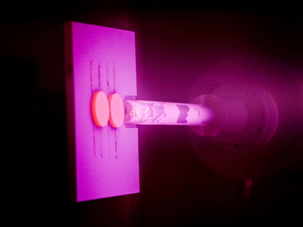
PVD is a cornerstone technique for depositing thin films. It encompasses a family of vacuum-based methods—thermal evaporation, electron beam (e-beam) evaporation, and sputtering—whereby material from a solid or liquid source (the target) is vaporized and transported to a substrate, condensing as a thin film. The PVD process is prized for its ability to deposit a wide array of materials, including metals, alloys, ceramics, and composite structures.
Key features of PVD include:
– High purity and density of coatings
– Precise control over film thickness and composition
– Ability to deposit multilayer and nanostructured films
– Suitability for a wide range of substrate materials
PVD sources have evolved to address the increasing demands for uniformity, scalability, and process flexibility. Advanced targets, vacuum boxes, and modular systems now enable large-area coatings and high-throughput operations, supporting industries from microelectronics to optics.
Atomic Layer Deposition (ALD)
ALD is a vapor-phase technique based on sequential, self-limiting surface reactions. In ALD, precursor gases are pulsed alternately into a vacuum chamber, reacting with the substrate surface one atomic layer at a time. This enables the deposition of ultra-thin films with atomic-scale control over thickness, exceptional conformality (even on 3D or porous substrates), and unparalleled uniformity.
Distinctive attributes of ALD are:
– Angstrom-level control over film thickness
– Excellent step coverage and conformality on complex geometries
– High-quality, pinhole-free films
– Precise stoichiometry and composition tuning
ALD is particularly valuable for creating barrier layers, dielectric films, and functional coatings in advanced electronic, optical, and energy devices.
The Genesis of Hybrid PVD–ALD Processes
Why Hybridize?
While PVD and ALD offer unique advantages, each technique has inherent limitations. PVD excels at rapid, large-area deposition of metals and alloys but can struggle with conformality on high-aspect-ratio or porous structures. ALD, conversely, is slow and often limited in the range of materials it can efficiently deposit, but it delivers outstanding conformality and film uniformity.
By integrating PVD and ALD into a hybrid process, engineers and scientists can leverage the best of both worlds—combining the throughput and versatility of PVD with the atomic precision and conformality of ALD. This hybridization opens new avenues for engineering multi-functional, high-performance coatings tailored to the most demanding applications.
Process Architectures
Hybrid PVD–ALD processes can be implemented in several configurations:
– **Sequential Processing:** PVD and ALD steps are performed in separate chambers, sometimes within cluster tools that allow vacuum transfer between modules.
– **In-situ Hybridization:** Advanced chambers enable both PVD and ALD steps without breaking vacuum, minimizing contamination and improving process efficiency.
– **Co-Deposition and Superlattice Formation:** Alternating PVD and ALD layers at the nanoscale to create superlattice structures with tunable properties.
Technical Advantages of Hybrid PVD–ALD Approaches
Enhanced Durability and Functionality
One of the foremost benefits of hybrid processes is the ability to produce coatings with superior durability and functionality. For example, a PVD metal layer can provide mechanical strength and conductivity, while an ALD dielectric or barrier layer imparts chemical inertness, corrosion resistance, or controlled electronic properties.
Engineered Multi-Layer and Composite Structures
Hybridization enables the design of multi-layer stacks and composite films that maximize the strengths of each technique. Examples include:
– **Barrier Layers:** PVD-deposited metal films encapsulated with ultra-thin ALD oxide or nitride layers prevent diffusion and improve corrosion resistance.
– **Superlattices:** Alternating PVD and ALD layers at the nanoscale can tune mechanical, optical, or electronic properties, enabling applications in photonics, sensors, and protective coatings.
– **Hybrid Crucibles and Targets:** Composite materials such as Mo-W-Cu laminates, or ceramics like yttria-stabilized zirconia, can be coated using both PVD and ALD to optimize chemical inertness and thermal fatigue resistance.
Improved Adhesion and Interface Engineering
ALD’s surface-controlled growth can be used to create adhesion-promoting interlayers between PVD films and substrates, addressing one of the persistent challenges in thin film engineering. This results in coatings with better mechanical integrity and longer service life, crucial for applications such as turbine blades, cutting tools, and microelectronic devices.
Superior Step Coverage and Conformality
Hybrid PVD–ALD is particularly advantageous for coating substrates with complex topographies, including high-aspect-ratio trenches, porous structures, and 3D architectures. PVD provides the bulk or functional layers, while ALD ensures uniform coverage in hard-to-reach areas, leading to performance enhancements in semiconductor devices, MEMS, and catalytic supports.
Applications Across Strategic Industries
Semiconductor and Microelectronics
In advanced semiconductor manufacturing, the demand for smaller, more densely packed features requires precise control over film thickness, composition, and interface quality. Hybrid PVD–ALD methods are increasingly used for:
– **Diffusion Barriers:** Tantalum or titanium nitride layers (via PVD) capped with ALD-deposited alumina or hafnia prevent copper migration in interconnects.
– **Gate Dielectrics:** ALD provides ultra-thin, high-κ dielectrics, while PVD delivers conductive gate metals.
– **Passivation Layers:** Combined processes create robust, pinhole-free passivation layers, enhancing device yield and reliability.
Optical and Photonic Coatings
Hybrid coatings enable precise manipulation of refractive index profiles, scratch resistance, and environmental stability for optical components. Applications include:
– **Anti-Reflective and High-Reflective Stacks:** Multilayer structures alternate PVD and ALD films for optimal optical performance.
– **Optical Information Storage:** Uniform, defect-free coatings are vital for data storage devices.
Aerospace and Automotive Engineering
Durability, thermal stability, and resistance to aggressive environments are paramount. Hybrid coatings provide:
– **Thermal Barrier Coatings (TBCs):** PVD-deposited bond coats topped with ALD ceramic layers (e.g., yttria-stabilized zirconia) offer superior resistance to oxidation and thermal cycling.
– **Wear-Resistant Layers:** Composite coatings extend the lifespan of engine parts, turbine blades, and cutting tools.
Energy and Catalysis
The energy sector leverages hybrid coatings for:
– **Protective Coatings for Batteries and Fuel Cells:** ALD layers improve chemical stability and cycle life; PVD films provide electrical conductivity.
– **Photovoltaic and Photocatalytic Devices:** Multi-layer coatings improve light absorption, charge separation, and environmental resistance.
Biomedical Devices and Implants
Medical devices demand biocompatibility, chemical inertness, and wear resistance. Hybrid coatings enable:
– **Corrosion-Resistant Barriers:** PVD metals with ALD oxide/nitride capping layers protect implants from bodily fluids.
– **Antimicrobial Surfaces:** Functional ALD layers can be added to PVD-coated implants to inhibit bacterial growth.
Advanced Materials and Composite Innovations
Hybrid Crucibles and Targets
Hybrid PVD–ALD processes are driving innovation in the design of crucibles and sputtering targets. Composite structures—such as Mo-W-Cu laminates or ceramic-coated metal crucibles—offer improved thermal fatigue resistance, chemical inertness, and reduced cross-contamination. These advances are critical for high-purity deposition of organics, aggressive halides, and rare-earth metals in next-generation device manufacturing.
Functional Composite Films
The ability to alternate between PVD and ALD enables the creation of functional composite films with tailored electrical, mechanical, and optical properties. For example, integrating rare-earth metals via PVD and capping with ALD oxides can produce films for advanced magnetics, photonics, and catalytic applications.
Process Control, Simulation, and Digital Manufacturing Integration
Simulation-Aided Design and Process Optimization
Recent trends emphasize the importance of simulation-aided design in optimizing hybrid PVD–ALD processes. Modeling tools now enable:
– **Prediction of Film Growth:** Simulate atomic-scale interactions and growth dynamics to optimize process recipes.
– **Stress and Strain Analysis:** Model multilayer stacks to predict mechanical behavior under thermal cycling.
– **Interface Engineering:** Visualize and tune interfaces at the atomic level for improved adhesion and performance.
Integration with Digital Manufacturing
Hybrid processes are being integrated with digital manufacturing systems, supporting:
– **Process Automation:** Real-time control and adjustment of process parameters based on in-situ diagnostics.
– **Data-Driven Optimization:** Machine learning algorithms analyze process data to optimize throughput, yield, and film quality.
– **Smart Coatings:** Coatings that respond to environmental conditions (temperature, humidity, chemical exposure) are being engineered using hybrid processes and digital feedback loops.
Strict Quality Control and Industrial Scalability
Meeting Industry Standards
To ensure reliability and reproducibility, hybrid PVD–ALD processes are governed by rigorous quality standards (e.g., ISO 9001, ISO 14001). This includes:
– **Material Purity:** Elimination of contamination during deposition, especially for high-purity organics and sensitive electronic materials.
– **Uniformity and Reproducibility:** Tight control over film thickness, stoichiometry, and interface quality across large substrates or batches.
– **Traceability:** Comprehensive documentation and monitoring throughout the production cycle.
Equipment Advances and Modularization
Industry is witnessing a shift toward high-capacity, modular vacuum systems that support hybrid processes:
– **Box Coaters with Interchangeable Liners:** Allow for rapid changeover and reduced downtime, crucial for high-throughput operations.
– **Cluster Tools:** Integrate multiple PVD and ALD modules, enabling seamless vacuum transfer and process integration.
– **Custom Machining and Bonding Services:** Enhanced flexibility in target and substrate design (e.g., custom backing plates, advanced bonding techniques) further supports hybrid process adoption.
Challenges and Solutions in Hybrid PVD–ALD Processes
Material Compatibility and Interface Engineering
A key challenge is ensuring compatibility between PVD and ALD materials, particularly at interfaces. Strategies include:
– **Surface Preparation:** In-situ plasma cleaning or pre-treatment to promote adhesion.
– **Intermediate Layers:** ALD nucleation layers between PVD films and difficult substrates.
Process Throughput and Cost
ALD’s inherently slow growth rates can limit throughput. Solutions are:
– **Spatial ALD:** Enables much faster deposition rates for large-area substrates.
– **Batch Processing and Modular Design:** Parallel processing and rapid tool changeover minimize downtime.
Thermal and Chemical Stability
Some applications require coatings to withstand extreme temperatures or aggressive chemicals. Hybridized ceramic and metallic layers, as well as advanced composite materials, are being developed to meet these demands.
Emerging Trends: Smart and Adaptive Coatings
Responsive and Self-Healing Coatings
Hybrid PVD–ALD processes are paving the way for smart coatings that respond to stimuli:
– **Self-Healing Films:** Incorporate ALD-grown reservoirs of healing agents within PVD layers to repair micro-cracks autonomously.
– **Sensing and Actuation:** Coatings that change optical or electrical properties in response to environmental changes enable new sensor and actuator technologies.
Green and Sustainable Manufacturing
With growing emphasis on sustainability, hybrid processes are being optimized for:
– **Material Efficiency:** Minimized waste through precise, layer-by-layer deposition.
– **Lower Temperature Processing:** ALD’s low-temperature capability reduces energy consumption and broadens substrate compatibility.
Case Studies: Real-World Impact of Hybrid PVD–ALD Processes
Protective Coatings for Engine Turbine Blades
Engine turbine blades are subjected to extreme thermal and mechanical stress. Hybrid coatings—combining PVD bond coats with ALD ceramic barrier layers—have demonstrated:
– **Extended Service Life:** Resistance to oxidation, corrosion, and thermal cycling.
– **Improved Mechanical Integrity:** Reduced crack propagation and spallation.
Semiconductor Diffusion Barriers
In advanced integrated circuits, copper interconnects are shielded by PVD tantalum or titanium nitride layers, capped with ALD alumina or hafnia. This hybrid approach:
– **Prevents Metal Diffusion:** Maintains device performance and reliability.
– **Enables Further Scaling:** Supports advanced node miniaturization.
Optical Components for Harsh Environments
Hybrid coatings on optical lenses and windows, alternating PVD metals and ALD oxides, result in:
– **Enhanced Scratch and Abrasion Resistance:** Prolonging optical component life.
– **Environmental Protection:** Preventing degradation from moisture, chemicals, or UV exposure.
Technical Recommendations for Adopting Hybrid PVD–ALD Processes
Process Selection and Customization
– **Assess Application Requirements:** Consider desired properties (mechanical, optical, electrical, chemical) and environmental demands.
– **Material and Stack Design:** Choose compatible PVD and ALD materials; optimize layer thicknesses and sequences.
– **Substrate Preparation:** Implement appropriate surface treatments for optimal adhesion and nucleation.
Equipment and Infrastructure
– **Invest in Modular, Flexible Systems:** Support both PVD and ALD in a single platform or cluster, with rapid changeover capability.
– **Ensure Robust Process Control:** Integrate in-situ diagnostics, real-time monitoring, and feedback control for consistent results.
– **Leverage Simulation Tools:** Use modeling for recipe development and process optimization.
Quality Assurance and Scalability
– **Adhere to Industry Standards:** Maintain strict quality controls for material purity, uniformity, and reproducibility.
– **Plan for Scale-Up:** Design processes and equipment with scalability in mind, enabling transition from prototype to production.
Collaborative Development and Prototyping
– **Engage with Material Experts:** Collaborate with suppliers of advanced targets, crucibles, and thin-film materials.
– **Prototype Early:** Develop and test hybrid coatings on pilot systems to refine process parameters before full-scale deployment.
– **Continuous Improvement:** Gather feedback from end-users and integrate lessons learned into process evolution.
Future Directions and Outlook
Hybrid PVD–ALD processes are poised to play a central role in the next generation of surface engineering and thin-film technologies. Ongoing research and development efforts are focused on:
– **Expanding Material Libraries:** Developing new precursors and target compositions to broaden the range of available coatings.
– **Accelerating Throughput:** Advancing high-speed ALD and co-deposition techniques.
– **Advancing Smart Coatings:** Implementing self-healing, responsive, and multifunctional films.
– **Digital Twin and AI Integration:** Leveraging digital twins and artificial intelligence for predictive process control and rapid innovation.
As the quest for high-performance, durable, and functional coatings intensifies across industries, hybrid PVD–ALD processes stand as a key enabling technology. Their ability to merge the speed and versatility of PVD with the atomic precision and conformality of ALD will continue to unlock new opportunities, pushing the boundaries of what is possible in advanced coatings.
Conclusion
The integration of PVD and ALD into hybrid processes represents a paradigm shift in surface engineering. By combining the complementary strengths of each method, hybrid PVD–ALD enables the creation of coatings with unmatched durability, functionality, and versatility. From protecting turbine blades and microelectronic devices to enabling smart sensors and sustainable manufacturing, the impact of hybrid coatings is profound and far-reaching.
Adopting hybrid PVD–ALD processes requires careful consideration of material compatibility, process integration, equipment investments, and quality assurance. Yet, the rewards—enhanced product performance, longer service life, and access to new markets—are substantial.
With continued innovation in materials, process control, and digital integration, hybrid PVD–ALD stands at the forefront of advanced coating technologies, ready to meet the challenges and seize the opportunities of the 21st century.