Introduction
Gallium Phosphide (GaP) wafers are single-crystal semiconductor substrates widely used in optoelectronics, high-frequency electronics, and photonic device research. As a III–V compound semiconductor, GaP offers a wide bandgap, high thermal stability, and favorable optical properties, making it particularly suitable for visible light-emitting devices and advanced epitaxial growth platforms.
GaP has long been utilized in red, orange, and green light-emitting diodes (LEDs), as well as in lattice-matched heterostructures for compound semiconductor engineering. Today, GaP wafers continue to serve both industrial-scale manufacturing and cutting-edge research applications.
Detailed Description
Gallium Phosphide is an indirect bandgap semiconductor with a bandgap of approximately 2.26 eV at room temperature. Its material characteristics make it especially valuable for optoelectronic devices operating in the visible spectrum and for integration with other III–V compounds.
Crystal Structure & Orientation
GaP wafers are typically grown using methods such as Liquid Encapsulated Czochralski (LEC) or Vertical Gradient Freeze (VGF), ensuring high crystalline uniformity and low defect density. Standard crystallographic orientations include:
(100) ±0.5°
(111)A / (111)B
Custom miscut angles available upon request
Precise orientation control is essential for epitaxial growth, ensuring consistent film morphology and device performance.
Electrical & Optical Properties
Wide bandgap enables operation at elevated temperatures.
High refractive index makes GaP suitable for integrated photonic applications.
Good chemical stability allows compatibility with standard semiconductor processing.
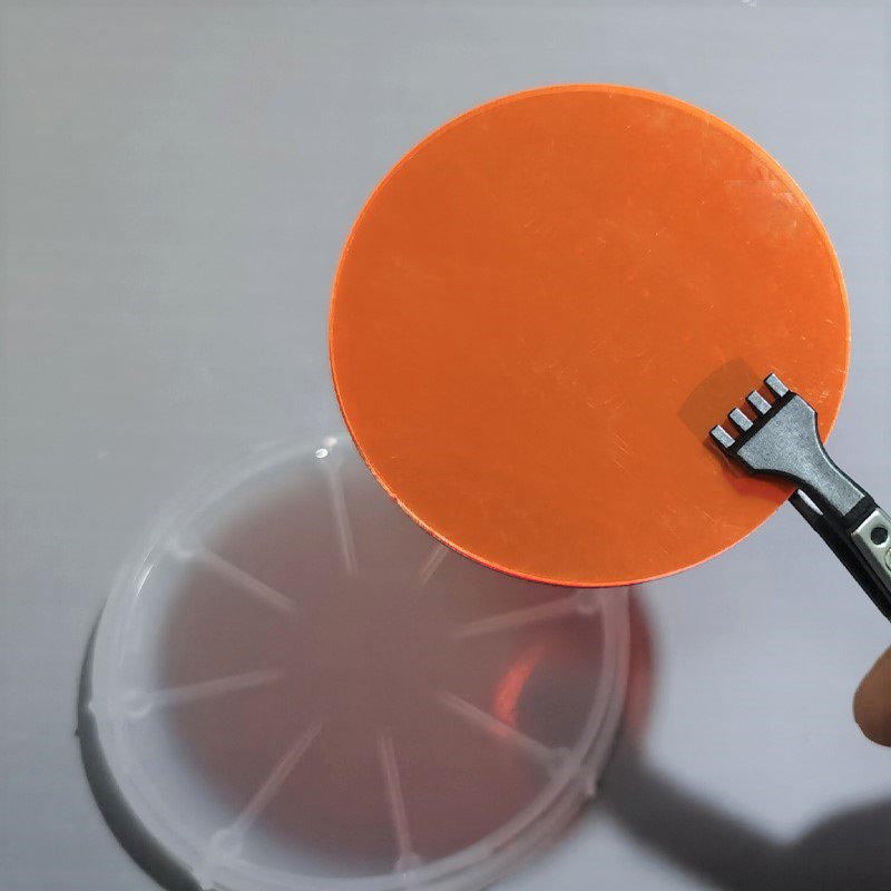
Doping options include n-type (commonly sulfur or tellurium doped) and p-type (commonly zinc doped), enabling tailored resistivity for device fabrication. Surface finish is typically epi-ready polished on one side (SSP) or double-side polished (DSP), depending on the application.
Applications
Gallium Phosphide wafers are widely used in the following industries and research fields:
Visible LEDs – Red, orange, and green emission devices
Photonic Devices – Waveguides, photonic crystals, and integrated optics
Epitaxial Substrates – For growth of GaAsP, AlGaInP, and other III–V compounds
Optical Sensors – Light detection and signal processing components
Power Electronics Research – Wide bandgap semiconductor studies
Microelectronics R&D – Heterostructure and junction device fabrication
GaP’s compatibility with lattice engineering makes it valuable in advanced heteroepitaxy systems for high-efficiency optoelectronic devices.
Technical Parameters
| Parameter | Typical Value / Range | Importance |
|---|---|---|
| Material | Gallium Phosphide (GaP) | Wide bandgap semiconductor |
| Diameter | 2″ – 4″ (custom sizes available) | Matches fabrication tools |
| Orientation | (100), (111)A/B | Controls epitaxial growth quality |
| Type | n-type / p-type | Enables device engineering |
| Resistivity | 0.01 – 10 Ω·cm (typical) | Determines electrical performance |
| Thickness | 350 – 500 µm (customizable) | Mechanical stability & handling |
| Surface Finish | SSP / DSP, Epi-ready | Ensures uniform thin film deposition |
Comparison with Related Materials
| Material | Key Advantage | Typical Application |
|---|---|---|
| GaP Wafer | Visible light emission capability | LEDs & photonics |
| GaAs | Direct bandgap, higher mobility | High-speed electronics |
| SiC | Wide bandgap, high thermal conductivity | Power electronics |
| Silicon (Si) | Low cost, mature processing | Integrated circuits |
Compared to silicon, GaP offers superior optical emission in the visible range. Compared to GaAs, GaP provides enhanced thermal and chemical robustness in specific optoelectronic configurations.
FAQ
| Question | Answer |
|---|---|
| Can GaP wafers be supplied with custom doping levels? | Yes, doping concentration and type (n or p) can be tailored to meet specific device requirements. |
| What wafer diameters are available? | Standard diameters include 2″ and 3″, with larger or custom sizes available upon request. |
| Are epi-ready surfaces available? | Yes, epi-polished surfaces suitable for MOCVD or MBE growth can be provided. |
| How are the wafers packaged? | Wafers are packed in cleanroom-compatible wafer boxes with vacuum-sealed protective packaging. |
| Can orientation and miscut be customized? | Yes, precise orientation and specific miscut angles can be manufactured to your specifications. |
Packaging
Our Gallium Phosphide (GaP) Wafers are meticulously tagged and labeled externally to ensure efficient identification and maintain high standards of quality control. We take great care to prevent any potential damage during storage and transportation, ensuring the wafers arrive in perfect condition.
Conclusion
Gallium Phosphide (GaP) Wafers provide a reliable, high-performance platform for visible optoelectronics, photonic integration, and compound semiconductor research. With customizable doping, orientation, surface finish, and wafer size options, GaP substrates offer flexibility for both industrial production and advanced R&D applications.
For detailed specifications and a quotation, please contact us at sales@thinfilmmaterials.com.

Reviews
There are no reviews yet.