Introduction
Gallium Arsenide (GaAs) is one of the most important III-V compound semiconductor materials used in optoelectronics, high-frequency devices, infrared technologies, and advanced semiconductor research. Unlike silicon, which dominates conventional microelectronics, GaAs offers a direct bandgap, high electron mobility, and strong performance advantages in applications where light emission, light detection, or high-speed electronic behavior is required.
In thin-film deposition, a Gallium Arsenide Sputtering Target serves as the material source for preparing GaAs-based films by physical vapor deposition. For researchers and engineers working with compound semiconductor thin films, the sputtering target is not simply a consumable item. Its purity, stoichiometry, density, surface condition, geometry, and bonding configuration can all influence deposition stability, process repeatability, and final film quality.
Because GaAs is a compound semiconductor containing arsenic, target selection and process planning require more attention than standard metallic sputtering targets. Buyers should consider not only the nominal material name, but also the required purity, Ga:As composition, target density, sputtering system compatibility, bonding needs, and documentation scope.
This article explains the properties, applications, and thin-film deposition considerations of GaAs sputtering targets and provides a practical guide for engineers selecting GaAs targets for research or production use.
What Is a Gallium Arsenide Sputtering Target?
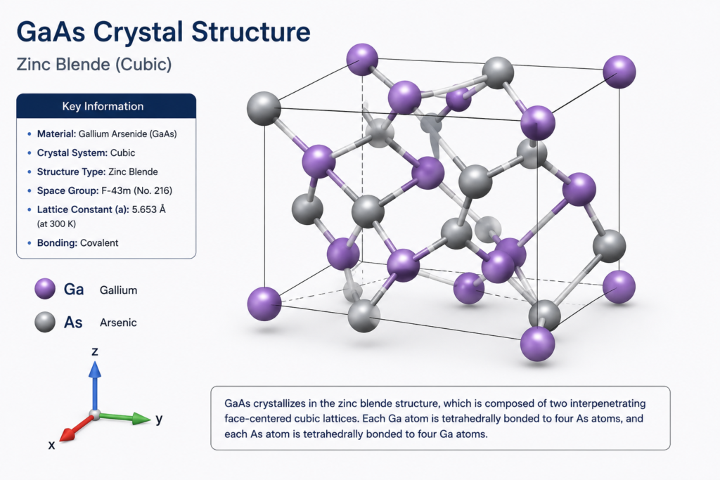
A Gallium Arsenide Sputtering Target is a solid GaAs source material used in magnetron sputtering systems to deposit gallium arsenide thin films. The target is typically installed inside a vacuum chamber, where energetic ions bombard the target surface and eject atoms or clusters that then deposit onto a substrate.
GaAs belongs to the III-V semiconductor family, where gallium is a group III element and arsenic is a group V element. This compound semiconductor structure gives GaAs properties that make it valuable in optoelectronic and high-frequency applications.
Compared with simple metal targets, compound semiconductor sputtering targets require more careful control because the film composition may be affected by sputtering parameters, preferential sputtering behavior, substrate temperature, and post-deposition treatment. Even when a stoichiometric GaAs target is used, the final film properties still depend strongly on the complete deposition process.
TFM supplies customized Gallium Arsenide Sputtering Targets in disc, plate, rectangular, bonded, and drawing-specific configurations for R&D and industrial thin-film deposition applications.
Suggested internal links:
- Gallium Arsenide Sputtering Target
- Compound Semiconductor Sputtering Targets
- Sputtering Target Bonding Service
Key Properties of Gallium Arsenide
Gallium arsenide is widely studied because it offers several properties that are difficult to achieve with traditional semiconductor materials.
Direct Bandgap Semiconductor Behavior
One of the most important features of GaAs is its direct bandgap. In a direct bandgap semiconductor, electrons can transition between energy states efficiently while emitting or absorbing photons. This makes GaAs highly useful for optoelectronic devices.
Because of this property, GaAs is commonly associated with:
- Light-emitting devices
- Laser diode structures
- Photodetectors
- Infrared devices
- Solar cell research
- Optical communication components
For thin-film researchers, GaAs sputtering targets provide a route to deposit GaAs-based films for device development, functional layer studies, and compound semiconductor experiments.
High Electron Mobility
GaAs is also valued for its high electron mobility. This makes it suitable for high-speed and high-frequency electronic applications, especially where signal response and carrier transport are important.
GaAs-based materials are frequently used in:
- RF devices
- Microwave electronics
- High-speed semiconductor structures
- Compound semiconductor research platforms
Although epitaxial growth methods such as MBE or MOCVD are often used for high-performance GaAs devices, sputtering remains valuable for thin-film research, multilayer structures, functional coatings, and non-epitaxial or application-specific deposition studies.
Compound Semiconductor Chemistry
GaAs is not a simple elemental semiconductor. Its performance depends on the controlled combination of gallium and arsenic. For this reason, the Ga:As ratio, target manufacturing method, and process environment must be considered carefully.
A GaAs sputtering target should be specified clearly as a gallium arsenide compound target, not as a mixture of separate gallium and arsenic sources unless a special co-sputtering process is being designed.
Typical Specifications of GaAs Sputtering Targets
Before purchasing a GaAs target, buyers should provide detailed specifications to avoid delays and mismatched quotations.
| Parameter | Typical Requirement | Why It Matters |
|---|---|---|
| Material | Gallium Arsenide, GaAs | Defines the compound semiconductor source material |
| Purity | 99.9%, 99.99%, or project-specific | Reduces unwanted impurity contribution to films |
| Composition | Stoichiometric GaAs or custom requirement | Supports intended film chemistry |
| Shape | Disc, plate, rectangular, custom | Must match sputtering cathode design |
| Diameter | 25–300 mm or custom | Determines holder compatibility |
| Thickness | 3–6 mm typical, custom available | Affects lifetime and mechanical stability |
| Density | High-density target preferred | Helps improve sputtering stability and reduce particles |
| Bonding | Unbonded or bonded to backing plate | Improves handling, support, and thermal contact |
| Surface Finish | Machined, ground, cleaned | Influences target conditioning and particle control |
| Documentation | CoA, composition data, dimensional report | Supports incoming quality control and traceability |
For compound semiconductor targets, it is especially important to confirm whether the target will be used for RF sputtering, DC sputtering, reactive sputtering, or system-specific deposition. The conductivity, target structure, and power mode compatibility should be reviewed before production.
Why Purity Matters in GaAs Sputtering Targets
Purity is one of the first specifications buyers usually ask about, but its importance depends on the application.
For GaAs thin-film research, impurities can influence:
- Electrical properties
- Optical absorption
- Carrier concentration
- Defect formation
- Interface behavior
- Film repeatability
For early-stage R&D, 99.9% purity may be sufficient in some cases. For more sensitive optoelectronic or semiconductor-related studies, 99.99% or project-specific impurity control may be required.
However, purity alone does not define target quality. A high-purity target with poor density, unstable surface condition, or unsuitable bonding may still cause sputtering problems. Buyers should treat purity as one part of a complete specification package.
Important impurity-related questions include:
- What purity level is required?
- Are metallic impurities critical?
- Are oxygen or carbon limits important?
- Is a CoA required?
- Is the film intended for optical, electrical, or semiconductor research?
Providing this information during RFQ helps the supplier recommend a suitable GaAs target grade.
Stoichiometry and Composition Control
For GaAs sputtering targets, stoichiometry is a major consideration. Since GaAs is a compound material, the ideal target composition is normally based on a controlled gallium-to-arsenic ratio.
In actual sputtering, the final film composition may not be exactly identical to the target composition. Film stoichiometry can be influenced by:
- Sputtering power
- Working pressure
- Target-to-substrate distance
- Substrate temperature
- Preferential sputtering behavior
- Re-sputtering effects
- Chamber background contamination
- Post-deposition annealing
This is why it is not enough to simply purchase a GaAs target and expect a final film to automatically meet all electrical and optical requirements. The target provides the source material, but film performance depends on the complete deposition process.
For sensitive applications, engineers should evaluate the process window carefully and perform film characterization after deposition.
Common characterization methods include:
- XRD for crystallinity
- SEM or AFM for surface morphology
- EDS or XPS for composition
- Optical transmission testing
- Electrical measurement
- Thickness and uniformity mapping
Target Density and Microstructure
Target density affects sputtering behavior, especially for brittle compound semiconductor materials.
A high-density GaAs sputtering target can help improve:
- Stable plasma behavior
- Uniform erosion
- Lower particle generation
- Better mechanical integrity
- More consistent deposition rate
Low-density targets may contain pores, weak grain boundaries, or microstructural defects that can increase particle formation during sputtering. For compound semiconductor targets, poor density may also increase the risk of cracking, chipping, or unstable erosion.
Target microstructure should be as uniform as possible. Large defects, visible cracks, edge chips, or inconsistent surface preparation may affect installation and sputtering performance.
For this reason, GaAs targets should be handled carefully during machining, inspection, packaging, and installation.
Bonded vs Unbonded GaAs Sputtering Targets
GaAs targets can be supplied as unbonded targets or bonded assemblies, depending on size, thickness, system design, and deposition conditions.
Unbonded GaAs Targets
Unbonded targets are suitable when:
- The target is small enough for direct installation
- Power level is moderate
- The cathode design supports the target directly
- Thermal load is manageable
- The target thickness provides sufficient mechanical strength
Unbonded targets may be simpler and more cost-effective for R&D systems.
Bonded GaAs Targets
Bonding is often considered when:
- The target is thin or fragile
- The target diameter is large
- Thermal contact must be improved
- The sputtering system requires a backing plate
- Installation stability is important
- The user wants to reduce cracking risk during operation
A copper backing plate can improve mechanical support and heat transfer. Bonding may be performed using indium bonding, elastomer bonding, or other system-appropriate methods depending on process temperature and power requirements.
For brittle materials like GaAs, bonded assemblies are often reviewed carefully before quotation. Buyers should provide backing plate drawings, cathode model information, cooling conditions, and any existing target photos when available.
Suggested internal link:
RF Sputtering Compatibility
GaAs is a compound semiconductor target, so RF sputtering is commonly evaluated for deposition. RF sputtering is often used when the target material is insulating or semiconducting, or when stable plasma operation with a compound target is required.
However, the best power mode depends on:
- Target conductivity
- Deposition equipment
- Target size
- Desired film properties
- Process atmosphere
- Power supply capability
Before selecting a GaAs target, buyers should confirm:
- RF or DC sputtering system
- Magnetron type
- Target diameter and thickness
- Cooling method
- Power range
- Substrate temperature
- Working gas
- Film thickness target
If the target is intended for a specific cathode design, the drawing or old target sample should be reviewed before production.
Thin-Film Deposition Considerations
Using a GaAs sputtering target successfully requires attention to both target quality and deposition process.
Target Conditioning
Before deposition, the target is usually pre-sputtered to remove surface contamination and stabilize the target surface. This step can help reduce early-stage particle release and improve film consistency.
For compound semiconductor targets, pre-sputtering time and power ramping should be selected carefully to avoid thermal shock.
Power Density
Excessive power density may increase the risk of target cracking, arcing, or particle generation. Power should be increased gradually, especially for bonded or brittle targets.
A stable deposition process usually requires balancing deposition rate with target safety.
Substrate Temperature
Substrate temperature strongly influences film morphology, crystallinity, and adhesion. For GaAs films, temperature may also affect composition and defect behavior. The best condition depends on the substrate material and final film requirement.
Working Pressure
Working pressure affects particle energy, mean free path, film density, and deposition rate. Lower pressure may increase particle energy, while higher pressure may change film morphology. The process should be optimized based on film performance requirements.
Post-Deposition Annealing
Some GaAs thin-film processes may require post-deposition annealing to improve crystallinity, reduce defects, or adjust film properties. Annealing conditions must be chosen carefully to avoid unwanted composition changes or interface reactions.
Applications of GaAs Sputtering Targets
GaAs sputtering targets are used in both academic and industrial research where compound semiconductor thin films are required.
Optoelectronic Devices
GaAs is widely associated with optoelectronic technologies because of its direct bandgap. GaAs thin films may be explored in light-emitting, light-detecting, and optical response applications.
Potential research areas include:
- Photodetectors
- Infrared response devices
- Light-emitting structures
- Optical sensors
- Semiconductor multilayers
RF and Microwave Research
GaAs-based materials are important in high-frequency electronics. While many commercial devices use epitaxial GaAs wafers, sputtered GaAs films may be studied in functional thin-film stacks, device structures, or experimental RF-related materials.
Solar Cell Research
GaAs is known for its strong photovoltaic potential. GaAs-based thin films and multilayer structures may be investigated for advanced solar cell concepts and optical absorption studies.
Semiconductor and III-V Materials Research
GaAs targets are also used in general compound semiconductor research, including:
- III-V semiconductor films
- Buffer or functional layers
- Thin-film multilayers
- Material screening
- Device development platforms
Sensors and Functional Coatings
GaAs thin films may be used in research involving optical, electrical, or infrared-sensitive behavior. The exact application depends on film quality, substrate, and device design.
GaAs Sputtering Target vs GaAs Wafer
Buyers sometimes confuse GaAs sputtering targets with GaAs wafers, but they serve very different roles.
| Item | Main Role | Typical Use |
|---|---|---|
| GaAs Sputtering Target | Deposition source material | Producing GaAs-based thin films by sputtering |
| GaAs Wafer | Substrate or device platform | Epitaxy, RF devices, optoelectronics, chip fabrication |
| GaAs Powder/Pieces | Raw or source material | Specialized synthesis, evaporation, or research use |
A sputtering target is consumed during deposition. A wafer is usually used as a substrate or semiconductor device platform. When requesting a quotation, buyers should clearly state whether they need a target, wafer, pellet, powder, or evaporation source.
GaAs vs GaN vs InP Sputtering Targets
GaAs is part of a broader family of compound semiconductor sputtering targets.
| Material | Key Feature | Typical Research Direction |
|---|---|---|
| GaAs | Direct bandgap III-V semiconductor | Optoelectronics, infrared devices, RF research |
| GaN | Wide-bandgap semiconductor | LEDs, UV devices, power electronics |
| InP | III-V semiconductor for photonics | Lasers, detectors, high-speed devices |
| AlN | Nitride semiconductor / ceramic material | Buffer layers, insulation, acoustic devices |
GaAs is often chosen when the research focus involves infrared response, optoelectronics, or high-frequency semiconductor behavior. GaN is preferred for wide-bandgap, UV, LED, and power-related studies. InP is often used in photonic and communication-related devices.
There is no single best III-V target for all applications. The correct choice depends on the intended film function and deposition route.
Handling, Safety, and Packaging Considerations
Because GaAs contains arsenic, handling and disposal should follow appropriate laboratory and industrial safety procedures. Users should avoid generating dust, inhaling particles, or contacting damaged material without proper protection.
GaAs sputtering targets should be:
- Carefully cleaned before packaging
- Protected from impact
- Sealed to reduce contamination
- Clearly labeled
- Packed with cushioning materials
- Stored in a dry and clean environment
For bonded targets, packaging should protect both the GaAs target surface and the backing plate interface.
TFM can provide export-safe packaging and labeling according to target size, shape, and shipping requirements.
How to Request a GaAs Sputtering Target Quote
To receive an accurate quotation, buyers should provide as much technical information as possible.
| RFQ Item | Information to Provide |
|---|---|
| Material | Gallium Arsenide, GaAs |
| Purity | 99.9%, 99.99%, or project-specific |
| Size | Diameter × thickness or L × W × thickness |
| Shape | Disc, rectangular, plate, custom geometry |
| Bonding | Unbonded or bonded to backing plate |
| Backing Plate | Copper, molybdenum, or system-specific if required |
| Sputtering System | Cathode model, holder type, power mode |
| Application | Optoelectronic, RF, infrared, semiconductor, R&D |
| Documents | CoA, dimensional inspection, bonding record |
| Quantity | Number of targets required |
For replacement targets, customers can provide:
- Old target photos
- Used backing plate photos
- Cathode model
- Drawing
- Installed height
- Cooling surface requirement
This helps avoid dimensional mismatch and improves quotation accuracy.
Frequently Asked Questions
What is a GaAs sputtering target used for?
A GaAs sputtering target is used as a source material for depositing gallium arsenide thin films by sputtering. These films are studied in optoelectronics, infrared devices, RF research, photovoltaic structures, sensors, and compound semiconductor applications.
Can GaAs sputtering targets be customized?
Yes. GaAs targets can be customized by purity, diameter, thickness, rectangular dimensions, bonding structure, backing plate design, and documentation requirements.
Is RF sputtering required for GaAs targets?
RF sputtering is commonly evaluated for compound semiconductor targets such as GaAs. However, the correct power mode depends on the target properties, system design, and deposition process.
Can GaAs targets be bonded to copper backing plates?
Yes. Bonded GaAs target assemblies can be supplied after technical review. Bonding may help improve mechanical support, thermal contact, and installation stability.
Does the film composition always match the target composition?
Not necessarily. Final GaAs film composition depends on sputtering parameters, substrate conditions, process pressure, temperature, and post-deposition treatment. Film characterization is recommended for critical applications.
What documents can be supplied with GaAs targets?
Depending on the order, TFM can provide CoA, composition information, dimensional inspection records, and bonding documentation for bonded assemblies.
Conclusion
Gallium Arsenide Sputtering Targets are important source materials for depositing GaAs-based thin films in compound semiconductor research, optoelectronics, infrared devices, RF applications, photovoltaics, and advanced functional materials development.
Because GaAs is a compound semiconductor, target selection requires careful review of purity, stoichiometry, density, target geometry, bonding, power mode, and process compatibility. A high-quality GaAs target can support stable deposition, but final film performance still depends on the complete sputtering process, substrate, and post-treatment conditions.
TFM supplies customized Gallium Arsenide Sputtering Targets for research and industrial thin-film deposition, including disc targets, rectangular targets, bonded assemblies, and drawing-specific configurations.
For detailed specifications and a quotation, please contact us at sales@thinfilmmaterials.com.