Neodymium Sputtering Target
Introduction
Neodymium Sputtering Targets are essential materials for producing functional thin films used in advanced electronics, photonics, magnetic devices, and energy technologies. As a rare-earth element with strong magnetic behavior and unique optical responses, neodymium supports high-performance coatings that require precise composition control and consistent deposition characteristics.
Detailed Description
The Neodymium Sputtering Target is produced from high-purity neodymium metal refined through vacuum melting or powder metallurgy. Because neodymium readily oxidizes, the entire manufacturing process—from raw material preparation to final machining—is carried out in controlled environments to ensure stability and surface cleanliness.
The target exhibits a dense, uniform microstructure with minimized porosity, enabling smooth erosion under DC or RF sputtering. This enhances the consistency of thin-film composition and reduces particulate formation during deposition. For high-power sputtering systems, neodymium can be supplied with copper or titanium backing plates to improve heat transfer and maintain dimensional stability throughout long deposition cycles.
Neodymium thin films are valuable in optical modulation layers, magneto-optic coatings, catalytic surfaces, and magnetic multilayer structures used in next-generation data storage and spintronic devices.
Applications
Neodymium sputtering targets are widely used in:
Semiconductor processing – magnetic multilayers, memory components, integrated thin-film structures
Optical coatings – selective absorption coatings, IR filters, photonic devices
Magnetic thin films – sensors, actuators, micro-magnetics research
Energy systems – catalytic surfaces, specialized battery components
Display and photonic devices – optical isolators, wavelength control films
R&D laboratories – alloy development, rare-earth compound studies, advanced coating trials
Technical Parameters
| Parameter | Typical Value / Range | Importance |
|---|---|---|
| Purity | 99.5% – 99.95% | High purity stabilizes optical and magnetic film performance |
| Diameter | 25 – 300 mm (custom) | Compatible with most commercial sputtering systems |
| Thickness | 3 – 10 mm | Determines sputtering lifetime and deposition rate |
| Bonding | Cu / Ti bonding plate | Improves cooling efficiency and mechanical stability |
| Density | ≥ 98% theoretical | Ensures uniform erosion and reduces defects |
Comparison with Related Materials
| Material | Key Advantage | Typical Application |
|---|---|---|
| Neodymium (Nd) | Strong magnetic response and optical effects | Magnetic multilayers, photonic coatings |
| Samarium (Sm) | High thermal stability | Magnetic sensors, energy devices |
| Dysprosium (Dy) | Coercivity enhancement | Spintronics, data storage |
| Aluminum (Al) | Cost-effective, reflective | General coatings, optical layers |
FAQ
| Question | Answer |
|---|---|
| Can the target be customized? | Yes. Purity, size, microstructure, and bonding options can be fully customized. |
| How do you package neodymium targets? | Vacuum-sealed with desiccant, foam protection, and export-grade cartons or wooden crates. |
| Is neodymium difficult to sputter? | It is reactive, but dense targets with proper bonding ensure stable sputtering. |
| Do you offer backing plates? | Yes—copper, titanium, indium bonding, and elastomer bonding options are available. |
| Which industries use this target? | Semiconductor fabrication, optics, magnetics, energy research, and academic R&D. |
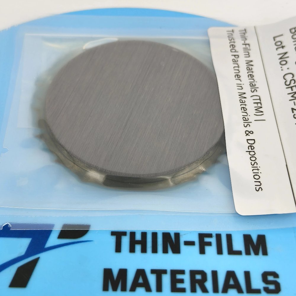
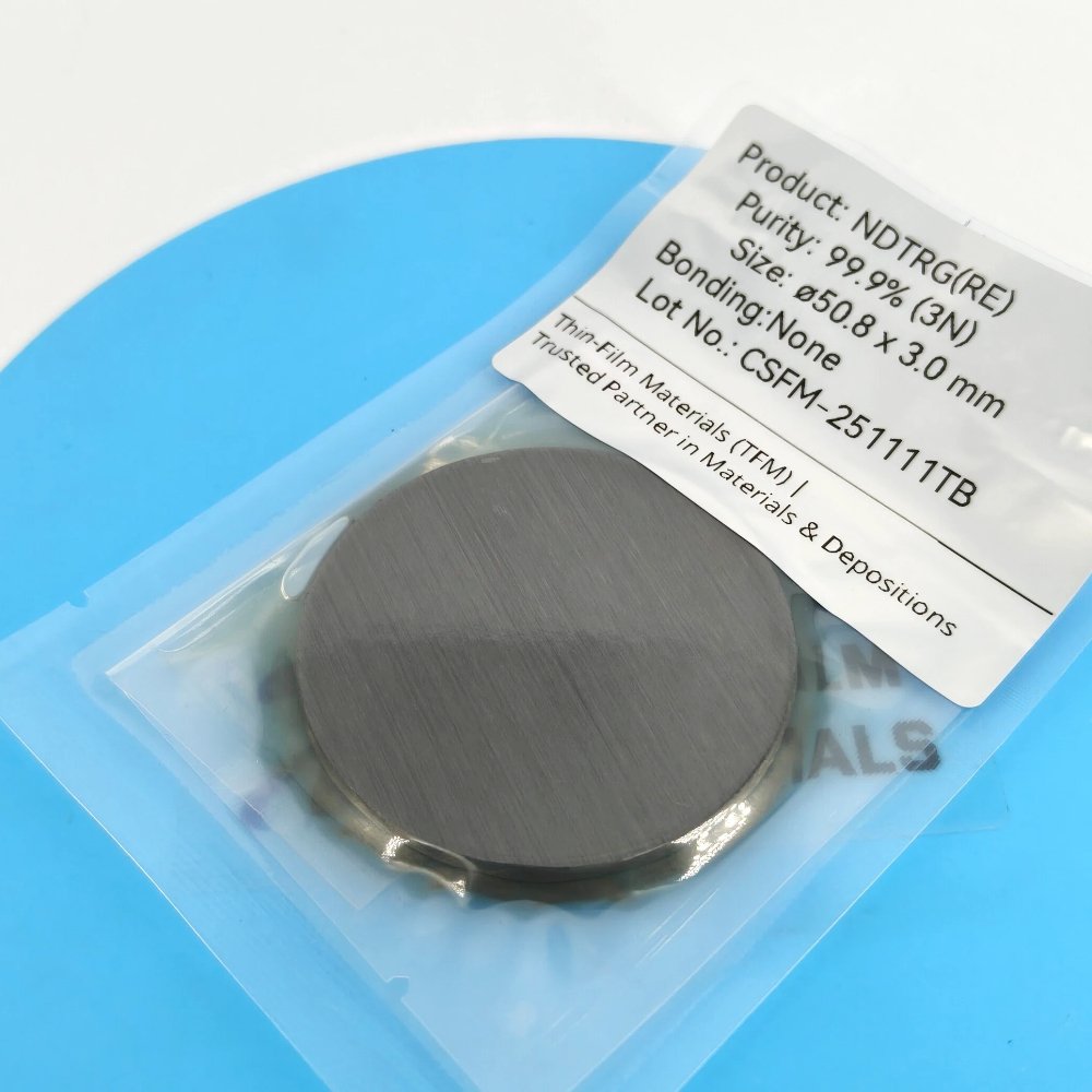
Packaging
Each Neodymium Sputtering Target is vacuum-sealed and clearly labeled. Protective layers and rigid external packaging prevent oxidation and mechanical damage during transportation. This ensures the target arrives in optimal condition for high-precision thin-film deposition.
Conclusion
With stable magnetic performance, strong reactivity control, and excellent deposition behavior, Neodymium Sputtering Targets offer reliable performance for semiconductor, optical, magnetic, and energy-related thin-film applications. Custom dimensions and bonding options are available to meet both R&D and production-scale requirements.
For detailed specifications or a quotation, please contact us at sales@thinfilmmaterials.com.


Reviews
There are no reviews yet.