
Niobium Silicide Sputtering Target
Introduction
Niobium Silicide (NbSi₂) Sputtering Target is a high-performance ceramic-metallic material designed for thin film deposition in semiconductors, electronics, and advanced research applications. Combining the refractory properties of niobium with the semiconducting and structural characteristics of silicon, NbSi₂ thin films exhibit excellent hardness, thermal stability, and oxidation resistance. This makes the material particularly valuable for protective coatings, microelectronics, and functional device research.
Detailed Description
Niobium Silicide sputtering targets are manufactured using high-purity NbSi₂ powder consolidated by hot pressing or vacuum sintering. The resulting targets feature dense microstructures, low porosity, and high purity, ensuring consistent sputtering rates and uniform thin film quality.
Chemical Formula: NbSi₂
Purity: 99.9% (3N) or higher on request.
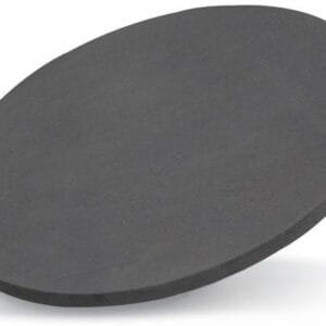
Appearance: Dark gray, ceramic-like solid.
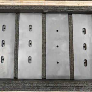
Forms & Dimensions: Available as circular (25–300 mm), rectangular, and custom designs. Typical thickness: 3–6 mm.
Bonding Options: Indium or elastomer bonding to copper/titanium back plates to enhance thermal management and minimize cracking.
Properties: High melting point (~1,950 °C), high hardness, stable in oxidizing environments, and good adhesion.
Applications
Niobium Silicide sputtering targets are applied in:
Semiconductors – Conductive and barrier layers in integrated circuits.
Protective Coatings – Wear-resistant and oxidation-resistant films.
Microelectronics – Thin films for transistors, diodes, and MEMS devices.
Optical & Functional Coatings – High-stability coatings for optical components.
R&D – Advanced studies in refractory silicides, superconductivity, and high-temperature materials.
Technical Parameters
| Parameter | Typical Value / Range | Importance |
|---|---|---|
| Purity | ≥ 99.9% | Ensures clean thin films with minimal contamination |
| Diameter | 25 – 300 mm (custom) | Compatible with a wide range of sputtering systems |
| Thickness | 3 – 6 mm | Influences deposition rate and sputtering stability |
| Bonding | Copper / Titanium backing | Enhances heat transfer and prevents target cracking |
| Melting Point | ~1,950 °C | High thermal stability for demanding applications |
Comparison with Related Materials
| Material | Key Advantage | Typical Application |
|---|---|---|
| Niobium Silicide (NbSi₂) | High hardness & oxidation resistance | Protective and functional coatings |
| Titanium Silicide (TiSi₂) | Low resistivity, good for contacts | Semiconductor interconnects |
| Molybdenum Silicide (MoSi₂) | Excellent high-temp oxidation stability | Heating elements, protective films |
FAQ
| Question | Answer |
|---|---|
| Can NbSi₂ targets be customized? | Yes, dimensions, thickness, and bonding can be tailored to system requirements. |
| What is the typical lead time? | Standard production time is 2–3 weeks depending on specifications. |
| Is NbSi₂ brittle? | Yes, it is a ceramic material and requires careful handling during installation. |
| How is it packaged? | Vacuum-sealed, cushioned with protective foam, and shipped in export-grade cartons or wooden crates. |
| Which industries use NbSi₂ the most? | Microelectronics, semiconductors, optics, and high-temperature materials R&D. |
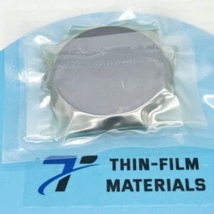
Packaging
Niobium Silicide sputtering targets are vacuum-sealed to prevent oxidation and contamination. Each unit is carefully packed in foam-protected cartons or wooden crates with clear labeling for traceability and safe handling.
Conclusion
Niobium Silicide Sputtering Targets combine refractory strength, thermal stability, and oxidation resistance, making them ideal for advanced thin film deposition in semiconductors, protective coatings, and R&D. With customizable purity, size, and bonding options, NbSi₂ targets are a reliable solution for both research and industrial production.
For detailed specifications and a quotation, please contact us at [sales@thinfilmmaterials.com].
Reviews
There are no reviews yet.