Introduction
Vanadium Tungsten Sputtering Targets (V/W) are advanced alloy targets used in physical vapor deposition (PVD) processes to create high-performance thin films. By combining the corrosion resistance and chemical stability of vanadium with the high melting point and mechanical strength of tungsten, V/W sputtering targets enable the deposition of films that perform reliably in demanding environments such as semiconductor manufacturing, optical coatings, and protective surface engineering.
These alloy targets are particularly valued for applications that require excellent thermal stability, controlled electrical conductivity, and resistance to wear or oxidation. As thin-film technologies continue to evolve in microelectronics, energy devices, and advanced coatings, Vanadium Tungsten sputtering targets provide a versatile material solution for producing functional coatings with tailored properties.
Detailed Description
Vanadium Tungsten Sputtering Targets are manufactured by combining high-purity vanadium and tungsten through advanced powder metallurgy or vacuum melting techniques. The resulting alloy structure offers improved stability compared with single-element targets while maintaining high sputtering efficiency and uniform film deposition.
The presence of tungsten contributes exceptional high-temperature stability and hardness, while vanadium enhances oxidation resistance, ductility, and adhesion characteristics in the resulting thin films. This combination allows V/W alloy coatings to maintain structural integrity under extreme operating conditions, including elevated temperatures and aggressive environments.
High-density targets with carefully controlled grain structures help ensure stable sputtering rates and consistent film composition throughout long deposition runs. Uniform microstructure and low porosity are essential to minimize particle generation during sputtering, which is critical in semiconductor and precision coating applications.
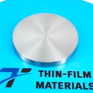
Vanadium Tungsten sputtering targets are typically available in various custom compositions, enabling engineers to optimize film properties such as electrical conductivity, mechanical hardness, or corrosion resistance. Targets can be manufactured in multiple shapes and sizes to match standard sputtering cathodes, including circular, rectangular, and rotatable configurations.
For improved thermal management and mechanical stability during high-power sputtering processes, V/W targets are often supplied with bonded backing plates made of copper or titanium. This bonding improves heat transfer from the target surface to the cooling system, helping maintain deposition stability and extending target service life.
Applications
Vanadium Tungsten sputtering targets are used across a variety of advanced thin-film technologies:
Semiconductor Manufacturing – Deposition of conductive or barrier layers in integrated circuits.
Protective Coatings – Hard, wear-resistant coatings for cutting tools and mechanical components.
Optical Thin Films – Functional coatings for optical filters, sensors, and specialized optical devices.
Energy Systems – Thin films used in fuel cells, energy conversion devices, and advanced batteries.
High-Temperature Electronics – Stable coatings for components operating under extreme thermal conditions.
Research and Development – Experimental alloy thin films and advanced materials studies.
Technical Parameters
| Parameter | Typical Value / Range | Importance |
|---|---|---|
| Purity | 99.9% – 99.99% | High purity improves film uniformity and electrical performance |
| Composition | Custom V/W ratios available | Allows tuning of film properties |
| Density | ≥ 95% theoretical density | Ensures stable sputtering behavior |
| Diameter | 25 – 300 mm (custom) | Compatible with various sputtering systems |
| Thickness | 3 – 6 mm | Influences sputtering lifetime and deposition stability |
| Bonding | Copper / Titanium backing plate | Improves thermal conductivity and mechanical stability |
Comparison with Related Materials
| Material | Key Advantage | Typical Application |
|---|---|---|
| Vanadium Tungsten | High-temperature stability and corrosion resistance | Semiconductor and protective coatings |
| Tungsten | Extremely high melting point and hardness | Wear-resistant and high-temperature coatings |
| Vanadium | Good oxidation resistance and adhesion | Functional and corrosion-resistant films |
FAQ
| Question | Answer |
|---|---|
| Can the Vanadium Tungsten Sputtering Target composition be customized? | Yes, different V/W ratios can be produced to achieve specific electrical or mechanical properties. |
| Are backing plates available? | Yes, copper or titanium backing plates are commonly used to enhance heat dissipation and target stability. |
| What sputtering methods are compatible with this target? | The target can be used in DC, RF, and magnetron sputtering systems depending on the application. |
| What industries commonly use V/W thin films? | Semiconductor manufacturing, advanced coatings, energy technologies, and research laboratories. |
| Can the target be manufactured in non-standard shapes? | Yes, circular, rectangular, and rotatable targets can be customized to fit specific sputtering equipment. |
Packaging
Our Vanadium Tungsten Sputtering Targets are meticulously tagged and labeled externally to ensure efficient identification and maintain high standards of quality control. Each target is carefully packaged using protective foam, vacuum sealing, and export-grade cartons or wooden crates to prevent contamination or mechanical damage during storage and transportation.
Conclusion
Vanadium Tungsten Sputtering Targets provide a reliable alloy solution for depositing high-performance thin films that require excellent thermal stability, corrosion resistance, and mechanical durability. With customizable compositions, precise manufacturing, and optional backing plate bonding, these targets support consistent deposition results in advanced thin-film applications.
For detailed specifications and a quotation, please contact us at sales@thinfilmmaterials.com.


Reviews
There are no reviews yet.