
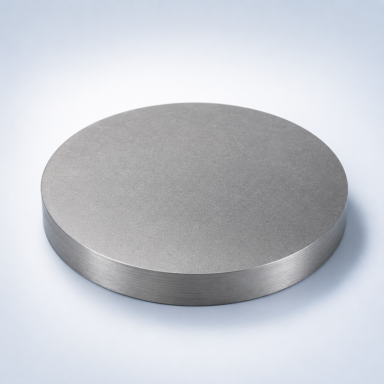
Product Overview
Antimony Doped Tin Oxide Sputtering Target (ATO Sputtering Target) is a conductive-oxide sputtering target used to deposit transparent or semiconducting functional thin films. In this material family, target density, dopant level, resistivity, sputtering mode, oxygen partial pressure, and substrate temperature can all influence the balance between film conductivity, optical transmission, composition, and microstructure.
Material and Deposition Characteristics
Conductive-oxide sputtering is strongly affected by target density, resistivity, dopant content, power density, working pressure, oxygen content, substrate temperature, and film thickness. RF magnetron sputtering is broadly applicable to ceramic targets, while sufficiently conductive grades may also be compatible with DC or pulsed-DC systems depending on equipment design. The process window should ultimately be tuned against measured film electrical and optical performance.
Technical Data
| Parameter | Typical Value / Range | Importance |
|---|---|---|
| Purity | 99.9% – 99.99% | Ensures consistent electrical and optical properties |
| Composition | SnO₂ doped with Sb (2–10 wt%) | Controls conductivity and transparency |
| Density | ≥ 95% theoretical density | Ensures stable sputtering performance |
| Diameter | 25 – 300 mm (custom) | Compatible with various sputtering systems |
| Thickness | 3 – 6 mm | Influences sputtering lifetime |
| Bonding | Copper / Titanium backing plate optional | Improves heat dissipation during sputtering |
| Material | Key Advantage | Typical Application |
|---|---|---|
| Antimony Doped Tin Oxide (ATO) | Stable conductive oxide with good transparency | Antistatic coatings and conductive films |
| Indium Tin Oxide (ITO) | Very high transparency and conductivity | Displays and touch panels |
| Fluorine Doped Tin Oxide (FTO) | Excellent thermal stability | Solar cells and glass coatings |
| Aluminum Doped Zinc Oxide (AZO) | Indium-free, cost-effective TCO | Photovoltaic devices |
| Question | Answer |
|---|---|
| What is the typical antimony doping level in ATO targets? | Typical Sb doping ranges from 2% to 10%, depending on the required conductivity and transparency. |
| What sputtering methods are suitable for ATO targets? | ATO sputtering targets are commonly used in RF magnetron sputtering systems for oxide film deposition. |
| What substrates are compatible with ATO coatings? | Glass, silicon wafers, ceramics, and polymer films are commonly used substrates. |
| Can ATO sputtering targets be customized? | Yes, target size, thickness, composition, and backing plate options can be customized. |
| What industries commonly use ATO coatings? | Electronics, solar energy, display technology, and optical coating industries. |
Typical Thin-Film Applications
- Transparent conductive oxide coatings for displays, photovoltaics, smart windows, sensors, and optoelectronics
- Thin-film electronics and transparent electrode development
- Projects balancing optical transmission, conductivity, and process compatibility
Target Configuration and Ordering Considerations
When requesting a quotation, provide target diameter or rectangular dimensions, thickness, purity or composition, required quantity, and whether a backing plate or bonded assembly is needed. For brittle ceramic or compound targets, it is useful to specify the cathode model, backing-plate material, preferred bonding method, operating power if known, and any density, tolerance, or inspection-document requirements. TFM can review drawings, old-target photos, and application details when custom dimensions are required.
Frequently Asked Questions
What are Antimony Doped Tin Oxide sputtering targets used for?
They are used to deposit transparent conductive or semiconducting oxide films for displays, photovoltaics, smart windows, sensors, and other thin-film electronic or optoelectronic applications.
Can Antimony Doped Tin Oxide targets be sputtered with RF or DC power?
RF sputtering is widely applicable to ceramic conductive-oxide targets. Depending on target resistivity and equipment capability, some grades may also be compatible with DC or pulsed-DC operation.
Why is target density important for Antimony Doped Tin Oxide?
Higher and more uniform density generally supports more stable erosion and can reduce pores, particles, local hot spots, and arc-related problems. Density should be considered together with microstructure and bonding quality.
How do oxygen partial pressure and power affect Antimony Doped Tin Oxide films?
These parameters can influence film composition, carrier concentration, resistivity, transparency, and microstructure. The process window should therefore be optimized against the actual film-performance targets.
Can the dopant level or composition of Antimony Doped Tin Oxide be customized?
Yes. The required composition should be stated clearly in the RFQ so that the target formulation and any acceptance criteria can be agreed before production.
What information should I provide to request a Antimony Doped Tin Oxide target quotation?
Please provide composition, purity basis, dimensions, quantity, planar or rotary format, backing requirement, cathode model if known, and any density, resistivity, optical, or documentation requirements.
Reviews
There are no reviews yet.