
Introduction
The Hafnium Silicide Sputtering Target (HfSi₂) is a refractory metal silicide target used in advanced thin-film deposition where thermal stability, low electrical resistivity, and excellent compatibility with silicon technologies are required. HfSi₂ is particularly valued in semiconductor and microelectronic applications as a contact, diffusion barrier, or functional layer in high-temperature environments.
With its combination of high melting point behavior and stable electrical performance, HfSi₂ has become an important material for both research laboratories and pilot-scale semiconductor processes.
Detailed Description
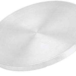
Hafnium Silicide sputtering targets are manufactured from high-purity hafnium and silicon through controlled alloying, reaction synthesis, and precision machining. The resulting target features uniform stoichiometry, dense microstructure, and consistent electrical properties, all of which are critical for reproducible sputtering performance and film quality.
Compared with pure hafnium or silicon targets, HfSi₂ offers improved thermal stability and lower contact resistance, making it suitable for high-temperature deposition and post-annealing processes. During magnetron sputtering, HfSi₂ targets demonstrate stable plasma behavior and predictable erosion profiles, enabling reliable thickness and composition control.
Targets can be supplied as monolithic silicide discs or bonded to copper or titanium backing plates to enhance heat dissipation and mechanical stability under higher sputtering power densities.
Applications
Hafnium Silicide sputtering targets are widely used in:
Semiconductor contacts and interconnect research
Diffusion barrier and adhesion layers
High-temperature thin-film electronics
Gate stack and CMOS-related materials research
Functional silicide thin films
Academic and industrial thin-film R&D
Technical Parameters
| Parameter | Typical Value / Range | Importance |
|---|---|---|
| Chemical Formula | HfSi₂ | Defines silicide functionality |
| Purity | 99.9% – 99.99% | Ensures electrical consistency |
| Target Diameter | 25 – 300 mm (custom) | Compatible with standard sputtering guns |
| Thickness | 3 – 6 mm (custom available) | Influences sputtering stability |
| Density | ≥ 99% of theoretical | Promotes uniform erosion |
| Backing Plate | Optional (Cu / Ti) | Improves thermal management |
| Deposition Method | DC / RF Magnetron Sputtering | Process flexibility |
Comparison with Related Silicide Targets
| Material | Key Advantage | Typical Application |
|---|---|---|
| Hafnium Silicide (HfSi₂) | High thermal stability, low resistivity | Semiconductor contacts |
| Titanium Silicide (TiSi₂) | Low resistivity | CMOS interconnects |
| Cobalt Silicide (CoSi₂) | Good silicon compatibility | Integrated circuits |
| Tantalum Silicide (TaSi₂) | High melting point | High-temperature electronics |
FAQ
| Question | Answer |
|---|---|
| Is HfSi₂ suitable for high-temperature processing? | Yes, it maintains stability during high-temperature deposition and annealing. |
| Is DC sputtering possible? | Yes, DC sputtering is commonly used for conductive silicide targets. |
| Is bonding recommended? | Bonded targets are recommended for larger sizes or higher power densities. |
| Can small R&D targets be supplied? | Yes, laboratory-scale sizes are available. |
| How is the target packaged? | Vacuum-sealed with protective cushioning to prevent oxidation or damage. |
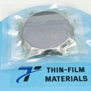
Packaging
Our Hafnium Silicide Sputtering Targets (HfSi₂) are meticulously vacuum-sealed and externally labeled to ensure accurate identification and strict quality control. Shock-absorbing, moisture-resistant packaging is used to protect the target during storage and international transportation.
Conclusion
The Hafnium Silicide Sputtering Target (HfSi₂) provides a reliable material solution for depositing thermally stable, low-resistivity silicide thin films used in advanced semiconductor and electronic applications. With customizable dimensions, stable sputtering behavior, and consistent material quality, HfSi₂ targets are well suited for both cutting-edge research and emerging production processes.
For detailed specifications and a quotation, please contact us at sales@thinfilmmaterials.com.

Reviews
There are no reviews yet.