
Niobium Silicide Sputtering Target
Introduction
The Niobium Silicide Sputtering Target (NbSi₂) is a specialized material engineered for thin film deposition, combining the refractory properties of niobium with the semiconducting and thermal stability characteristics of silicon. This target material is widely used in semiconductor research, microelectronics, protective coatings, and advanced optical devices where high temperature resistance and stable electrical performance are required.
Detailed Description
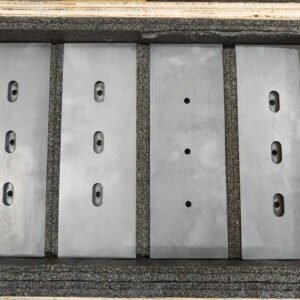
Niobium silicide targets are generally produced by powder metallurgy techniques such as hot pressing or hot isostatic pressing (HIP) to achieve high density and homogeneity. With a typical composition of Niobium Disilicide (NbSi₂), the target exhibits strong covalent bonding, leading to excellent hardness, oxidation resistance, and thermal conductivity.
Key features include:
High Purity (≥99.9%): Ensures clean thin films with minimal contamination.
Strong Oxidation Resistance: Stable in high-temperature and oxidative environments.
Mechanical Hardness: Produces durable films suitable for protective and wear-resistant coatings.
Electronic Properties: Suitable for microelectronic and semiconductor device fabrication.
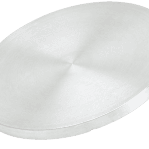
Tailored Geometry: Available in planar and rotary forms, with bonding options for better thermal management.
Applications
Niobium Silicide Sputtering Targets are used across multiple advanced industries:
Semiconductors: Deposition of thin films for transistors, integrated circuits, and diffusion barriers.
Microelectronics: Metallization layers and functional coatings for devices.
Protective & Decorative Coatings: Hard coatings for cutting tools, optical instruments, and wear-resistant surfaces.
Energy & Photonics: Thin films for sensors, optical coatings, and high-temperature components.
R&D and Universities: Thin film studies in materials science, superconductivity, and nanotechnology.
Technical Parameters
| Parameter | Typical Value / Range | Importance |
|---|---|---|
| Purity | 99.9% – 99.99% | Higher purity ensures thin film reliability |
| Composition | NbSi₂ | Provides balance of hardness and oxidation resistance |
| Diameter | 25 – 300 mm (customizable) | Matches sputtering system requirements |
| Thickness | 3 – 6 mm | Influences deposition rate |
| Bonding | Copper / Titanium backing | Improves heat dissipation and target stability |
Comparison with Related Materials
| Material | Key Advantage | Typical Application |
|---|---|---|
| Niobium Silicide (NbSi₂) | High-temperature stability & hardness | Semiconductor coatings, wear protection |
| Pure Niobium (Nb) | Excellent ductility & conductivity | Superconductors, electronics |
| Silicon (Si) | Semiconductor properties | Integrated circuits, photonics |
FAQ
| Question | Answer |
|---|---|
| Can the target size be customized? | Yes, both planar and rotary targets can be tailored to specific system dimensions. |
| What bonding options are available? | Copper or titanium backing plates are commonly used for thermal management. |
| What is the delivery time? | Typically 3–4 weeks depending on order size and customization. |
| How is it packaged? | Targets are vacuum-sealed with protective foam and shipped in export-safe crates. |
| Which industries use it most? | Semiconductor, optics, energy, microelectronics, and R&D institutions. |
Packaging
Each Niobium Silicide Sputtering Target is securely vacuum-packed or argon-protected to prevent contamination. External labeling includes purity, dimensions, lot number, and composition to ensure traceability and quality control. Packaging is reinforced to withstand long-distance transport.
Conclusion
The Niobium Silicide Sputtering Target delivers a reliable solution for thin film deposition where high-temperature performance, oxidation resistance, and mechanical durability are essential. Its versatility across semiconductors, optics, and protective coatings makes it a valuable material for advanced research and industrial applications.
For detailed specifications and a quotation, please contact us at sales@thinfilmmaterials.com.

Reviews
There are no reviews yet.