Introduction
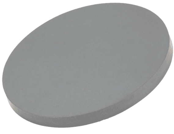
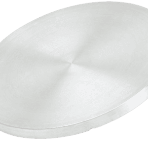
Hafnium Boride (HfB₂) Sputtering Target is an ultra-high-temperature ceramic (UHTC) material known for its exceptional hardness, high melting point, and outstanding thermal and chemical stability. With a melting point above 3000 °C and excellent electrical conductivity compared to many ceramics, HfB₂ is widely used in advanced protective coatings, aerospace materials research, and high-temperature functional films. As a sputtering target, HfB₂ enables deposition of dense boride-based thin films designed for extreme environments.
Detailed Description
Our Hafnium Boride Sputtering Targets are manufactured from high-purity HfB₂ powders using advanced consolidation and sintering techniques to achieve high density and structural uniformity. Precise control of the Hf:B ratio is critical to maintaining the diboride phase, which directly influences hardness, oxidation resistance, and electrical performance in the deposited film.
The targets exhibit a dense microstructure with minimal porosity, reducing particle ejection and ensuring stable plasma conditions during sputtering. Due to its electrical conductivity, HfB₂ can typically be used with DC sputtering systems, although RF sputtering is also compatible depending on equipment configuration. Targets are available in circular, rectangular, or custom geometries and can be supplied unbonded or bonded to copper backing plates for improved heat dissipation during high-power operation.
Applications
Hafnium Boride Sputtering Targets are widely used in demanding thin film applications, including:
Ultra-high-temperature protective coatings
Wear-resistant and hard coatings
Aerospace and hypersonic material research
Diffusion barrier and conductive ceramic layers
Plasma-facing and high-heat-flux components
Advanced boride and UHTC thin film development
Technical Parameters
| Parameter | Typical Value / Range | Importance |
|---|---|---|
| Chemical Composition | HfB₂ | Determines ultra-high-temperature stability |
| Purity | 99.5% – 99.9% | Minimizes impurity-related defects |
| Diameter | 25 – 200 mm (custom available) | Compatible with sputtering systems |
| Thickness | 3 – 6 mm | Influences target lifetime |
| Density | ≥ 95% theoretical | Improves plasma stability |
| Electrical Conductivity | Conductive ceramic | Enables DC sputtering |
| Bonding | Unbonded / Cu backing (optional) | Enhances thermal management |
Comparison with Related Boride Materials
| Material | Key Advantage | Typical Application |
|---|---|---|
| HfB₂ | Extreme temperature resistance | Aerospace & UHT coatings |
| ZrB₂ | High melting point & oxidation resistance | Thermal protection systems |
| TiB₂ | Excellent hardness & conductivity | Wear-resistant coatings |
| HfC | Ultra-high melting point | Extreme environment coatings |
FAQ
| Question | Answer |
|---|---|
| Is HfB₂ suitable for high-temperature coatings? | Yes, it is specifically valued for ultra-high-temperature applications. |
| Can DC sputtering be used? | Yes, HfB₂ is electrically conductive and compatible with DC sputtering. |
| Are custom sizes available? | Yes, diameter, thickness, and bonding options can be tailored. |
| How is the target packaged? | Vacuum-sealed with protective foam and export-grade cartons or crates. |
Packaging
Our Hafnium Boride (HfB₂) Sputtering Targets are carefully vacuum-sealed and labeled to ensure traceability and protection against contamination. Export-grade packaging safeguards the targets during storage and international transportation.
Conclusion
Hafnium Boride (HfB₂) Sputtering Target provides a robust solution for depositing ultra-high-temperature, wear-resistant, and conductive boride thin films. With high density, controlled composition, and customizable configurations, it is well suited for aerospace, energy, and advanced materials research applications.
For detailed specifications and a quotation, please contact us at sales@thinfilmmaterials.com.


Reviews
There are no reviews yet.