
Introduction
Titanium Selenide sputtering targets are layered chalcogenide materials widely used in advanced thin-film research, particularly in low-dimensional physics, optoelectronics, and energy-related applications. Owing to their unique electronic structure and strong electron–phonon interactions, titanium selenide thin films are of growing interest for charge density wave (CDW) studies, thermoelectric devices, and next-generation electronic materials.
Detailed Description
Titanium Selenide, most commonly TiSe₂, is a transition-metal dichalcogenide (TMD) with a layered crystal structure. Within each layer, titanium atoms are sandwiched between selenium layers, while weak van der Waals forces hold adjacent layers together. This structure enables anisotropic electrical transport and makes TiSe₂ particularly attractive for two-dimensional material research and ultrathin film fabrication.
Our Titanium Selenide sputtering targets are produced from high-purity titanium and selenium through controlled synthesis, vacuum melting or solid-state reaction, and high-density consolidation. The resulting targets exhibit excellent compositional uniformity, high density, and good mechanical integrity, ensuring stable sputtering behavior and reproducible film stoichiometry.
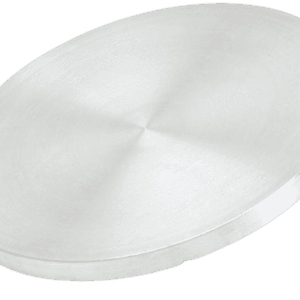
These targets are compatible with RF sputtering and, depending on system configuration and target conductivity, pulsed-DC sputtering. Planar disc targets are available in standard diameters, with optional bonding to copper backing plates to enhance heat dissipation and reduce thermal stress during deposition. Custom compositions, dimensions, and bonding options can be provided to meet specific research and pilot-scale requirements.
Applications
Titanium Selenide sputtering targets are commonly used in the deposition of thin films for:
Charge density wave (CDW) and correlated electron studies
Two-dimensional (2D) material and layered semiconductor research
Thermoelectric thin films and energy materials
Optoelectronic and infrared-related devices
Fundamental research on transition-metal dichalcogenides
Academic and industrial R&D in advanced chalcogenide materials
Technical Parameters
| Parameter | Typical Value / Range | Importance |
|---|---|---|
| Material | Titanium Selenide (TiSe₂) | Defines electronic & structural behavior |
| Purity | 99.9% – 99.99% | Minimizes impurity-induced defects |
| Crystal Structure | Layered TMD | Enables anisotropic properties |
| Diameter | 1″ – 4″ (custom available) | Fits standard sputtering cathodes |
| Thickness | 3 – 6 mm | Influences target lifetime |
| Density | ≥ 95% of theoretical | Ensures stable sputtering rate |
| Backing Plate | Optional Cu | Improves thermal management |
Comparison with Related Materials
| Material | Key Advantage | Typical Application |
|---|---|---|
| Titanium Selenide (TiSe₂) | CDW behavior, layered structure | 2D materials, electronics |
| Titanium Disulfide (TiS₂) | Higher conductivity | Energy storage, electronics |
| Molybdenum Diselenide (MoSe₂) | Direct bandgap in thin layers | Optoelectronics |
| Tungsten Diselenide (WSe₂) | Strong spin–orbit coupling | Valleytronics |
FAQ
| Question | Answer |
|---|---|
| Is Titanium Selenide suitable for RF sputtering? | Yes, RF sputtering is commonly used for TiSe₂ targets. |
| Can target size and thickness be customized? | Yes, dimensions and bonding options can be tailored. |
| Are bonded targets available? | Yes, copper-bonded targets are available upon request. |
| What research fields most commonly use TiSe₂ films? | 2D materials, CDW physics, thermoelectrics, and optoelectronics. |
Packaging
Our Titanium Selenide Sputtering Targets are meticulously tagged and labeled externally to ensure efficient identification and strict quality control. Each target is vacuum-sealed and protected with shock-absorbing materials to prevent contamination or mechanical damage during storage and transportation.
Conclusion
Titanium Selenide sputtering targets provide reliable composition control, stable sputtering performance, and high thin-film quality for advanced chalcogenide and layered-material research. With flexible customization options and consistent manufacturing quality, these targets are an excellent choice for cutting-edge thin-film and 2D material applications.
For detailed specifications and a quotation, please contact us at sales@thinfilmmaterials.com.


Reviews
There are no reviews yet.