Introduction
The Aluminum Telluride Sputtering Target (Al₂Te₃) is a compound semiconductor material used in thin film deposition processes for electronic, optoelectronic, and research applications. Aluminum telluride belongs to the family of III–VI compound semiconductors and has attracted increasing attention due to its unique electrical and optical properties. When deposited as a thin film through magnetron sputtering or other physical vapor deposition (PVD) techniques, Al₂Te₃ can serve as a functional material in semiconductor devices, photonic systems, and advanced research on chalcogenide materials.
Because of its tunable electronic structure and compatibility with other telluride-based compounds, aluminum telluride thin films are often explored in infrared technologies, thermoelectric materials research, and compound semiconductor development.
Detailed Description
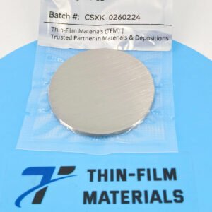
Aluminum Telluride sputtering targets are manufactured using high-purity aluminum and tellurium sources through controlled synthesis and advanced sintering or hot-pressing processes. These techniques ensure the formation of a dense, homogeneous target with consistent stoichiometry, which is critical for stable sputtering performance and uniform thin film deposition.
Al₂Te₃ exhibits semiconductor behavior with a band structure suitable for optoelectronic and infrared-related applications. The compound combines the lightweight, conductive characteristics of aluminum with the semiconducting and photonic properties of tellurium. As a result, aluminum telluride films can provide useful electrical and optical characteristics for specialized thin film devices.
In thin film deposition systems, aluminum telluride targets enable the growth of compound semiconductor layers with controlled composition and thickness. Maintaining the correct Al-to-Te ratio is particularly important for achieving the desired electrical properties and crystal structure. High-density targets help minimize particle generation during sputtering and ensure stable deposition rates.
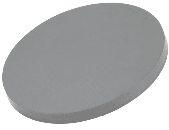
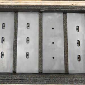
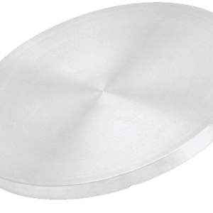
Depending on system requirements, Al₂Te₃ sputtering targets may be supplied as planar targets or bonded targets with copper backing plates, which improve thermal conductivity and mechanical stability during high-power sputtering operations.
Applications
Aluminum Telluride sputtering targets are used in several advanced research and technology fields:
Compound semiconductor thin films used in electronic and optoelectronic devices
Infrared and photonic materials research involving telluride-based compounds
Thermoelectric material studies where tellurium-containing compounds play a role
Thin film electronics requiring precise control of semiconductor composition
Photodetectors and optical sensors in specialized research environments
Academic and industrial R&D exploring new chalcogenide materials
Technical Parameters
| Parameter | Typical Value / Range | Importance |
|---|---|---|
| Purity | 99.9% – 99.99% | High purity ensures reliable semiconductor film properties |
| Chemical Formula | Al₂Te₃ | Determines compound stoichiometry and electronic structure |
| Diameter | 25 – 300 mm (custom) | Compatible with common sputtering systems |
| Thickness | 3 – 6 mm | Influences sputtering stability and target lifetime |
| Density | ≥ 95% theoretical density | Improves sputtering efficiency and film uniformity |
| Bonding | Copper backing plate / Indium bonded | Enhances heat transfer and structural stability |
Comparison with Related Materials
| Material | Key Advantage | Typical Application |
|---|---|---|
| Aluminum Telluride (Al₂Te₃) | Semiconductor properties with telluride-based functionality | Optoelectronic and thermoelectric research |
| Aluminum Oxide (Al₂O₃) | Excellent dielectric properties | Insulating thin films |
| Tellurium (Te) | Strong thermoelectric and semiconductor behavior | IR detectors and thermoelectric materials |
FAQ
| Question | Answer |
|---|---|
| Can the Al₂Te₃ sputtering target be customized? | Yes. Diameter, thickness, and bonding configurations can be customized to match different sputtering systems. |
| Which sputtering methods are compatible with this target? | Aluminum Telluride targets can be used in RF magnetron sputtering and other PVD deposition methods suitable for compound semiconductors. |
| Are bonded targets available? | Yes. Targets can be bonded to copper backing plates using indium or other bonding techniques to improve heat dissipation. |
| What purity levels are typically available? | Standard purities range from 99.9% to 99.99% depending on application requirements. |
| What substrates can Al₂Te₃ films be deposited on? | Thin films can be deposited on silicon wafers, glass, ceramics, and other semiconductor substrates. |
Packaging
Our Aluminum Telluride Sputtering Target (Al₂Te₃) products are meticulously tagged and labeled externally to ensure efficient identification and maintain high standards of quality control. Each target is carefully packaged using vacuum-sealed bags, protective foam, and export-safe cartons or wooden crates. These measures prevent oxidation, contamination, and mechanical damage during storage and transportation, ensuring that the sputtering targets arrive in excellent condition.
Conclusion
The Aluminum Telluride Sputtering Target (Al₂Te₃) provides a reliable material solution for depositing high-quality semiconductor and telluride-based thin films. Its balanced combination of aluminum’s structural properties and tellurium’s semiconductor characteristics makes it valuable for optoelectronic research, thermoelectric materials development, and advanced thin film technologies.
With customizable dimensions, high-density manufacturing, and stable sputtering performance, Al₂Te₃ sputtering targets are well suited for both industrial production and research applications.
For detailed specifications and a quotation, please contact us at sales@thinfilmmaterials.com.
Reviews
There are no reviews yet.