Germanium Antimony Telluride Sputtering Target Description
The Germanium Antimony Telluride (GeSbTe) Sputtering Target is used in thin-film deposition processes, especially in the semiconductor industry. Sputtering, a type of physical vapor deposition (PVD), involves bombarding a solid target with high-energy ions to deposit thin films onto a substrate.
GeSbTe is a compound semiconductor material known for its unique properties, making it ideal for various applications. It is widely used in phase-change random access memory (PRAM) devices due to its ability to transition between amorphous and crystalline states at different temperatures, enabling efficient data storage and retrieval. Additionally, GeSbTe-based thin films are employed in optical storage media, including rewritable CDs, DVDs, and Blu-ray discs.
Germanium Antimony Telluride Sputtering Target Specifications
| Compound Formula | Ge2Sb2Te5 |
| Molecular Weight | 322 g/mol (GeSbTe) / 1026.8 (GeSbTe – Ge2Sb2Te5) |
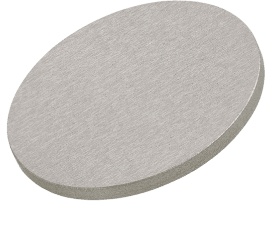
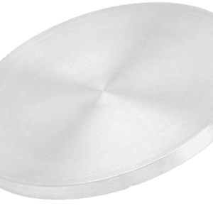
| Appearance | Silvery-gray metallic target |
| Melting Point | >600℃ |
| Density | 6.35 g/cm3 |
| Available Sizes | Dia.: 1.0″, 2.0″, 3.0″, 4.0″, 5.0″, 6.0″ Thick: 0.125″, 0.250″ |
Germanium Antimony Telluride Sputtering Target Handling Notes
Indium bonding is recommended for Germanium Antimony Telluride (GeSbTe) Sputtering Targets due to the material’s inherent brittleness and low thermal conductivity, which can make it less suitable for traditional sputtering methods. Indium bonding helps mitigate these issues by improving thermal conductivity and reducing the risk of thermal shock during the sputtering process.
Germanium Antimony Telluride Sputtering Target Application
Germanium Antimony Telluride (GeSbTe) Sputtering Targets are not typically used for applications requiring pure silicon films. Instead, they are specifically employed in phase-change memory devices and other applications that benefit from GeSbTe’s unique ability to switch between amorphous and crystalline states. These targets are used in the production of optical storage media, such as CDs, DVDs, and Blu-ray discs, as well as in some electronic and semiconductor devices.
Germanium Antimony Telluride Sputtering Target Packaging
Our Germanium Antimony Telluride Sputtering Targets are meticulously handled during storage and transportation to ensure that the quality of the products is maintained in their original condition.
Get Contact
TFM offers Germanium Antimony Telluride Sputtering Targets in various forms, purities, sizes, and prices. We specialize in high-purity thin film deposition materials with optimal density and minimal grain sizes, which are ideal for semiconductor, CVD, and PVD applications in display and optics. Contact Us for current pricing on sputtering targets and other deposition materials that are not listed.


Reviews
There are no reviews yet.