Copper(I) Sulfide Sputtering Targets Description
Copper(I) Sulfide Sputtering Target is a specialized material utilized in sputter deposition to create thin films of copper sulfide on various substrates. Sputter deposition is a prevalent technique in the production of electronic and optoelectronic devices, solar cells, and other applications requiring thin films with precise characteristics.
Copper sulfide materials are valuable in the manufacture of semiconductors, photovoltaic devices, and sensors. During the sputtering process, high-energy ions bombard the Copper(I) Sulfide Sputtering Target, causing atoms or molecules to be ejected. These ejected particles then deposit onto a substrate, forming a thin film of copper sulfide. The sputtering process allows for precise control over the film’s thickness and composition.
Related Products: Copper Sputtering Target, Copper (II) Selenide Sputtering Target, Copper Indium Sputtering Target
Copper(I) Sulfide Sputtering Targets Specifications
| Compound Formula | Cu2S |
| Molecular Weight | 159.16 |
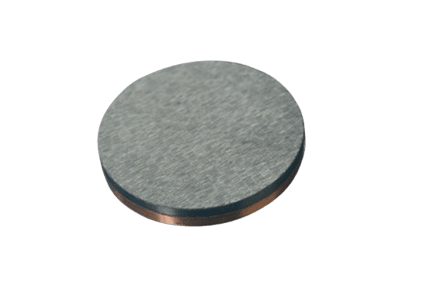
| Appearance | Black solid |
| Melting Point (℃) | 1130 |
| Boiling Point (℃) | N/A |
| Density (g/cm3) | 5.6 |
| Available Sizes | Dia.: 1.0″, 2.0″, 3.0″, 4.0″, 5.0″, 6.0″ Thick: 0.125″, 0.250″ |
Copper(I) Sulfide Sputtering Targets Application
Copper(I) Sulfide Sputtering Target is utilized in the fabrication of semiconductors, photovoltaic devices, and sensors.
Copper(I) Sulfide Sputtering Targets Packaging
Our Copper(I) Sulfide Sputtering Targets are meticulously handled during storage and transportation to ensure they retain their original quality.
Get Contact
TFM offers Copper(I) Sulfide Sputtering Targets in various forms, purities, sizes, and prices. We specialize in high-purity thin film deposition materials with optimal density and minimal grain sizes, which are ideal for semiconductor, CVD, and PVD applications in display and optics. Contact Us for current pricing on sputtering targets and other deposition materials that are not listed.


Reviews
There are no reviews yet.