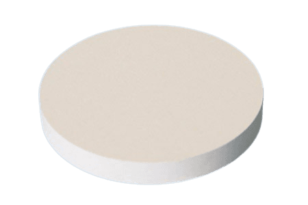
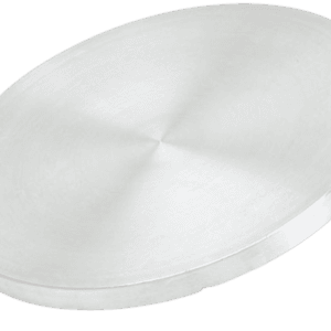
Germanium Disulphide Sputtering Target Description
TFM offers Germanium Disulphide Sputtering Targets, crafted from premium-grade materials to ensure superior performance and reliability in thin-film deposition. Our targets feature a unique Germanium and Disulphide composition, providing high electrical conductivity, a high melting point, and excellent chemical stability. These attributes make them ideal for applications in microelectronics, solar cells, and other advanced thin-film processes. TFM’s Germanium Disulphide Sputtering Targets meet the stringent requirements of both research and manufacturing professionals, supporting precise material control and high-quality results.
Related Product: Germanium Sputtering Target, Germanium Sulfide Sputtering Target
Germanium Disulphide Sputtering Target Specifications
| Compound Formula | GeS2 |
| Molecular Weight | 136.77 |
| Appearance | White Target |
| Melting Point | 800 °C |
| Density | 2.94 g/cm3 |
| Available Sizes | Dia.: 1.0″, 2.0″, 3.0″, 4.0″, 5.0″, 6.0″ Thick: 0.125″, 0.250″ |
Germanium Disulphide Sputtering Target Handling Notes
Indium bonding is recommended for Germanium Disulphide Sputtering Targets due to the material’s brittleness and low thermal conductivity, which can pose challenges during sputtering. The use of indium bonding helps mitigate these issues, enhancing sputtering performance and extending the target’s lifespan. This material’s low thermal conductivity and susceptibility to thermal shock necessitate careful handling to maintain its integrity and performance.
Germanium Disulphide Sputtering Target Application
- Microelectronics: Used in sputter coating for fabricating electronic devices and integrated circuits. The high thermal and electrical conductivity of the target material ensures performance and reliability in microelectronics.
- Solar Cells: Applied in the preparation of thin film solar cells, where precise control of film thickness and composition enhances photovoltaic conversion efficiency.
- Sensors and Detectors: Utilized to create photoelectric sensors and detectors due to their high photoconductive properties, enabling the detection of light, radiation, and other signals.
- Optical Devices: Employed in the manufacture of optical films such as transmittance enhancement films, reflective films, and filters, which improve the performance of optical devices.
- Composites and Ceramics: Integrated with other materials to produce composites and ceramics, achieving specific physical and chemical properties tailored for various applications.
Germanium Disulphide Sputtering Target Packaging
Our Germanium Disulphide Sputtering Target is meticulously handled throughout storage and transportation to ensure it arrives in pristine condition, maintaining the highest quality standards.
Get Contact
TFM offers Germanium Disulphide Sputtering Targets in various forms, purities, sizes, and prices. We specialize in high-purity thin film deposition materials with optimal density and minimal grain sizes, which are ideal for semiconductor, CVD, and PVD applications in display and optics. Contact Us for current pricing on sputtering targets and other deposition materials that are not listed.

Reviews
There are no reviews yet.