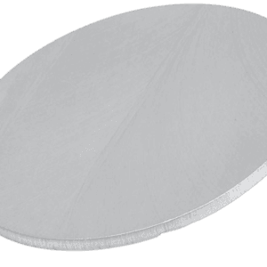
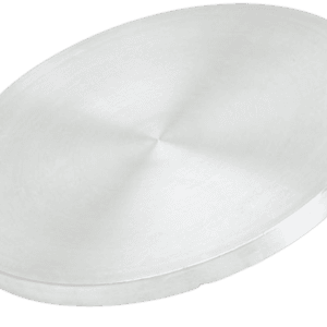
Silicon Phosphorous Sputtering Target
Introduction
The Silicon Phosphorous (Si–P) Sputtering Target is a semiconductor-grade alloy material designed for thin film deposition applications that require controlled n-type doping. By combining high-purity silicon with phosphorous, this target provides stable electrical characteristics and excellent film uniformity, making it indispensable in the production of semiconductor devices, photovoltaic cells, and microelectronic components.
Detailed Description
Silicon doped with phosphorous (Si:P) is a well-established n-type material in semiconductor technology. Phosphorous atoms introduce free electrons into the silicon lattice, enhancing electrical conductivity while maintaining the crystalline integrity and optical transparency of the deposited film.
The Si–P sputtering target is manufactured through precision melting, vacuum casting, and high-temperature sintering processes to ensure uniform dopant distribution and high density. This allows consistent sputtering behavior and reliable control over film resistivity and composition.
Key Features:
High purity (up to 99.999%) to ensure low defect density.
Stable dopant concentration for precise control of electrical properties.
Excellent uniformity and adhesion in deposited thin films.
Compatible with both RF and DC magnetron sputtering systems.
Available in a range of phosphorus concentrations (commonly 0.5–5 at.%).
Applications
Silicon Phosphorous sputtering targets are used in:
Semiconductors and microelectronics – n-type doped layers, transistor gates, and conductive interlayers.
Photovoltaics – doped silicon films for solar cell electrodes.
Thin film transistors (TFTs) – channel and contact layer formation.
Optoelectronic coatings – transparent conductive or semiconductor films.
R&D – semiconductor doping and advanced material studies.
Technical Parameters
| Parameter | Typical Value / Range | Importance |
|---|---|---|
| Composition | Si–P (0.5–5 at.% P) | Defines electrical conductivity |
| Purity | 99.99% – 99.999% | Reduces contamination for semiconductor use |
| Density | ≥ 2.33 g/cm³ (near theoretical) | Ensures uniform sputtering performance |
| Diameter | 25 – 300 mm (custom) | Fits standard sputtering systems |
| Thickness | 3 – 10 mm | Balances sputtering rate and target life |
| Backing Plate | Copper / Molybdenum | Improves heat dissipation and bonding strength |
Comparison with Related Materials
| Material | Key Advantage | Typical Application |
|---|---|---|
| Silicon Phosphorous (Si–P) | Controlled n-type doping & stability | Semiconductors, photovoltaics |
| Silicon Boron (Si–B) | p-type doping | Complementary semiconductor layers |
| Pure Silicon (Si) | High purity, intrinsic layer | Base material for electronics |
| Silicon Germanium (Si–Ge) | Tunable bandgap and strain control | High-speed electronics |
FAQ
| Question | Answer |
|---|---|
| Can the phosphorus concentration be customized? | Yes, from 0.5 to 5 at.% depending on electrical requirements. |
| Is the target suitable for both DC and RF sputtering? | Yes, it performs well in both systems. |
| How are the targets bonded? | Typically with copper or molybdenum backplates. |
| What purity levels are offered? | 4N to 5N purity levels are standard. |
| How are the targets packaged? | Vacuum-sealed with desiccant, cushioned, and shipped in export-safe crates. |
Packaging
Each Silicon Phosphorous Sputtering Target is carefully vacuum-sealed in cleanroom conditions, labeled for full traceability, and packed with anti-static and foam protection. Export packaging ensures the target remains free of oxidation and physical damage during transport.
Conclusion
The Si–P sputtering target combines the superior semiconducting properties of silicon with precise phosphorous doping to deliver stable, conductive, and uniform thin films. It is a cornerstone material for modern semiconductor and photovoltaic device fabrication, providing excellent control over electrical and structural characteristics.
For detailed specifications and quotations, please contact us at [sales@thinfilmmaterials.com].


Reviews
There are no reviews yet.