Generic selectors
Exact matches only
Search in title
Search in content
Post Type Selectors

ST0996 Tungsten Niobium Sputtering Target, W/Nb

Chemical FormulaW/Nb
Catalog No.ST0996
CAS Number
Purity99.9%, 99.95%, 99.99%, 99.995%, 99.999%
ShapeDiscs, Plates, Column Targets, Step Targets, Custom-made

With our extensive expertise in materials science, TFM offers Tungsten Niobium Sputtering Targets of exceptional purity. We are dedicated to providing cost-effective solutions tailored to meet the specific requirements of nanotechnology and thin-film deposition.

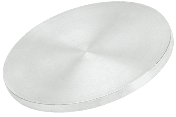
Tungsten Niobium Sputtering Target Description

Tungsten Niobium Sputtering Targets are advanced materials designed for thin-film deposition processes, leveraging the exceptional properties of both tungsten and niobium. These targets feature high melting points, excellent thermal conductivity, and outstanding mechanical strength. They offer exceptional stability, durability, and corrosion resistance, making them ideal for use in semiconductor manufacturing, optical coatings, and aerospace applications. Tungsten Niobium Sputtering Targets ensure precise and reliable film deposition, which enhances device performance, improves optical properties, and increases wear resistance. They are crucial for achieving high-quality thin films in various advanced technologies.

Related Product: Tungsten Sputtering Target, Cobalt Tungsten Sputtering Target

Tungsten Niobium Sputtering Target Specifications

Compound FormulaW/Nb
Molecular Weight276.86
AppearanceSilver Metallic Target
Available SizesDia.: 1.0″, 2.0″, 3.0″, 4.0″, 5.0″, 6.0″

Thick: 0.125″, 0.250″

Tungsten Niobium Sputtering Target Handling Notes

Indium bonding is recommended for the Tungsten Niobium Sputtering Target due to certain characteristics that make it challenging for direct sputtering, such as its brittleness and low thermal conductivity. The material’s low thermal conductivity and susceptibility to thermal shock further highlight the need for proper bonding to ensure optimal performance during sputtering.

Tungsten Niobium Sputtering Target Application

Semiconductor Manufacturing: Tungsten Niobium Sputtering Targets are used in producing integrated circuits, microchips, and other electronic devices. They allow for the precise deposition of thin films for interconnects, barrier layers, and contact materials, ensuring reliable electrical performance.

Optical Coatings: These targets are employed in fabricating optical coatings for lenses, mirrors, and filters. The films deposited exhibit high reflectivity, low absorption, and excellent adhesion, which enhance optical performance and durability.

Aerospace and Defense: In the aerospace and defense sectors, Tungsten Niobium Sputtering Targets are used to coat components like turbine blades, fuel cells, and thermal barrier coatings. Their high melting point and mechanical strength make them suitable for extreme operating conditions.

Energy Storage: Tungsten Niobium Sputtering Targets are utilized in creating thin films for energy storage devices such as lithium-ion batteries and supercapacitors. The films enhance electrode performance, resulting in higher energy density and improved cycling stability.

Research and Development: These targets are valuable for scientific research and development, aiding in the study of material properties, exploration of new thin-film deposition techniques, and development of advanced technologies.

Tungsten Niobium Sputtering Target Packaging

We meticulously handle our Tungsten Niobium Sputtering Target during storage and transportation to ensure it remains in its original, high-quality condition.

Get Contact

TFM offers Tungsten Niobium Sputtering Targets in a variety of forms, purities, and sizes. We specialize in producing high-purity physical vapor deposition (PVD) materials with maximum density and minimal average grain sizes, making them ideal for use in semiconductor applications, chemical vapor deposition (CVD), and PVD processes for display and optical technologies.

Reviews

There are no reviews yet.

Be the first to review “ST0996 Tungsten Niobium Sputtering Target, W/Nb”

Your email address will not be published. Required fields are marked *

Related Products

FAQ

It’s the source material (in solid form) used in sputter deposition to eject atoms or molecules that then form a thin film on a substrate.

Targets can be pure metals (e.g., gold, copper, aluminum), ceramics (e.g., Al₂O₃, SiO₂, TiO₂), alloys, or composites—chosen based on the film’s desired properties.


They are produced by processes such as melting/casting for metals or sintering (often with hot isostatic pressing) for ceramics and composite targets to ensure high density and purity.


In a vacuum chamber, a plasma (typically argon) bombards the target, ejecting atoms that travel and condense on a substrate, forming a thin film.


Key factors include the target’s purity, density, grain structure, and the sputtering yield (i.e. how many atoms are ejected per incident ion), as well as operating conditions like power density and gas pressure.


Operators monitor target erosion (often by measuring the depth of the eroded “race track”) or track total energy delivered (kilowatt-hours) until it reaches a threshold that can compromise film quality.


Fragile materials (such as many ceramics or certain oxides) and precious metals often require a backing plate to improve cooling, mechanical stability, and to allow thinner targets that reduce material costs.


DC sputtering is used for conductive targets, while RF sputtering is necessary for insulating targets (like many oxides) because it prevents charge buildup on the target’s surface.


In reactive sputtering, a reactive gas (e.g., oxygen or nitrogen) is introduced to form compound films on the substrate, but it may also “poison” the target surface if not carefully controlled.


Many manufacturers prefer to control raw material quality by sourcing their own powders; using external powders can risk impurities and inconsistent target properties.


Targets should be stored in clean, dry conditions (often in original packaging or re-wrapped in protective materials) and handled with gloves to avoid contamination, ensuring optimal performance during deposition.

Deposition rate depends on factors such as target material and composition, power density, working gas pressure, substrate distance, and the configuration of the sputtering system (e.g., magnetron design).

 
Shopping Cart
Scroll to Top