 MSDS File
Introduction
Lead (Pb) evaporation materials are widely used in vacuum deposition processes for producing functional metallic and compound thin films. Due to its relatively low melting point and stable evaporation behavior, lead is particularly suitable for thermal evaporation techniques, enabling uniform coating formation in applications ranging from electronics to radiation shielding layers.
Detailed Description
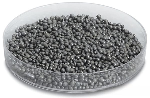
Lead evaporation materials are typically supplied in the form of pellets, granules, shots, or custom-cut pieces to match various evaporation sources such as resistive boats, crucibles, or electron beam systems. With a melting point of approximately 327°C, lead can be efficiently evaporated using thermal evaporation, making it a cost-effective choice for many thin film processes.
High-purity Pb materials are essential for achieving consistent film quality, especially in semiconductor and research applications. The softness and ductility of lead allow for easy handling and shaping, while its high density contributes to stable evaporation rates and good film coverage.
In addition, lead can be used as a precursor for compound film deposition (e.g., lead-based chalcogenides or perovskite materials) through co-evaporation or reactive deposition techniques. Careful control of evaporation rate and chamber conditions is necessary to ensure uniform film thickness and composition.
Key features include:
Low melting point for efficient thermal evaporation
Stable evaporation behavior with controllable deposition rates
High density for uniform film formation
Available in multiple forms (pellets, granules, shots, pieces)
Suitable for both pure metal films and compound film preparation
Applications
Lead evaporation materials are widely used in:
Thin film electronics and semiconductor research
Radiation shielding coatings and protective layers
Infrared and optoelectronic materials (e.g., Pb-based compounds)
Perovskite and chalcogenide thin film deposition
Battery and energy-related research
General laboratory vacuum coating processes
Technical Parameters
| Parameter | Typical Value / Range | Importance |
|---|---|---|
| Chemical Symbol | Pb | Defines material identity |
| Purity | 99.9% – 99.999% | Ensures film consistency |
| Form | Pellets / Granules / Shots / Pieces | Matches evaporation source |
| Particle Size | 1 – 10 mm (typical) | Affects evaporation stability |
| Melting Point | ~327°C | Enables thermal evaporation |
| Density | 11.34 g/cm³ | Influences deposition rate |
| Evaporation Method | Thermal / E-beam | Process compatibility |
Comparison with Related Materials
| Material | Key Advantage | Typical Application |
|---|---|---|
| Pb | Low melting point, easy evaporation | General thin films |
| Sn | Lower toxicity alternative | Electronics coatings |
| Bi | High density, unique electronic properties | Thermoelectrics |
| PbTe | Infrared and thermoelectric properties | IR detectors |
FAQ
| Question | Answer |
|---|---|
| What evaporation method is best for Pb? | Thermal evaporation is commonly used due to its low melting point. |
| Can Pb be used for compound film deposition? | Yes, it is often used in co-evaporation for lead-based compounds. |
| What forms are available? | Pellets, granules, shots, and custom shapes are available. |
| Is high purity necessary? | Yes, especially for semiconductor and research applications. |
| Which industries use Pb evaporation materials? | Electronics, optics, energy research, and laboratory coating. |
Packaging
Our Lead Evaporation Materials are meticulously tagged and labeled externally to ensure efficient identification and maintain high standards of quality control. We take great care to prevent contamination and mechanical damage during storage and transportation, ensuring the materials arrive in excellent condition.
Conclusion
Lead (Pb) evaporation materials provide a practical and efficient solution for thin film deposition, offering stable evaporation characteristics and broad application versatility. With customizable forms and high purity options, they are well-suited for both industrial and research environments.
For detailed specifications and a quotation, please contact us at sales@thinfilmmaterials.com.
Ordering Table
| Material | Size | Quantity | Purity | Part Number |
| Lead | 1mm - 4mm Shot | 100 g | 99.999% | EVMPB503MMD |
| Lead | 1mm - 4mm Shot | 200 g | 99.999% | EVMPB503MMH |
| Lead | 1mm - 4mm Shot | 1 kg | 99.999% | EVMPB503MMKG |
| Lead | 1mm - 4mm Shot | 500 g | 99.999% | EVMPB503MMT |


Reviews
There are no reviews yet.