

 MSDS File
Selenium Evaporation Material Description
Selenium, represented by the chemical symbol Se, is a non-metallic element found in the fourth period and group VI A (the 34th element) of the periodic table. It serves various purposes, including as a photosensitive material, a catalyst in the electrolytic manganese industry, and an essential nutrient for animals and plants. Selenium also functions as a semiconductor and is widely used in photocells.
High-purity selenium evaporation materials are essential for producing high-quality deposited films in various deposition processes. TFM specializes in manufacturing these materials with purities up to 99.9999%, ensuring product reliability through stringent quality assurance procedures.

Selenium Evaporation Material Specification
| Material Type | Selenium |
| Symbol | Se |
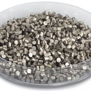
| Color/Appearance | Gray, Metallic Luster, Non-Metallic |
| Melting Point | 217 °C |
| Density | 4.79 g/cm3 |
| Thermal Conductivity | 0.00519 W·m-1·K-1 (25°C) |
| Thermal Expansion | 37 µm/(m·K) (25°C) |
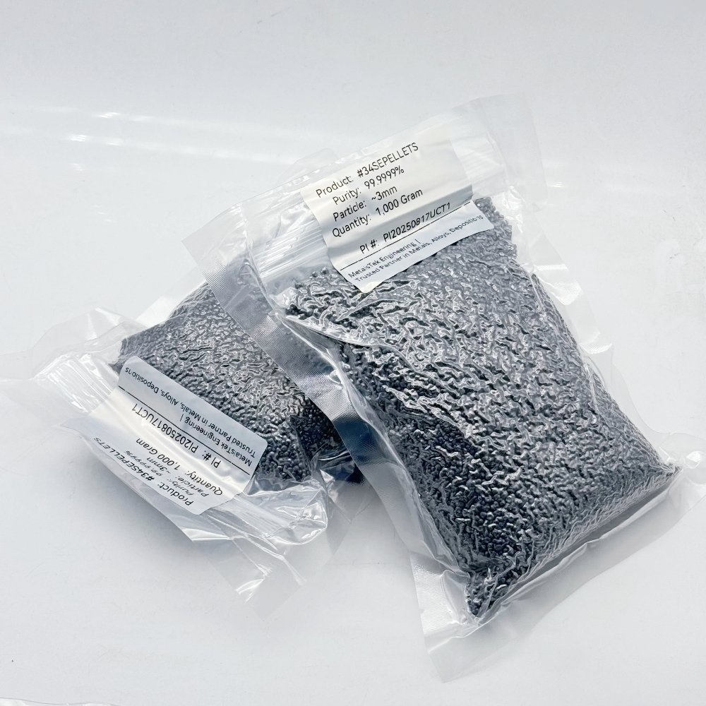
| Synonyms | Se Pellets, Se Pieces, Se Evaporation Pellet, Selenium Pellets, Selenium Pieces, Selenium Evaporation Pellet |
Selenium Evaporation Material Application
- Employed in deposition processes such as semiconductor deposition, chemical vapor deposition (CVD), and physical vapor deposition (PVD).
- Used in optics for various applications, including enhancing wear protection, creating decorative coatings, and advancing display technologies.
Selenium Evaporation Material Packaging
We handle our selenium evaporation materials with the utmost care to avoid any damage during storage and transportation. This meticulous approach ensures that the quality of our products is maintained in their original condition.
Get Contact
TFM offers selenium evaporation materials in a variety of forms, purities, sizes, and price points. We specialize in high-purity e-beam evaporation materials, designed for optimal density and minimal average grain sizes. For up-to-date pricing on evaporation pellets and other deposition materials not listed, please contact us directly.


Reviews
There are no reviews yet.