 MSDS File
Introduction
N-type Silicon Evaporation Materials (Si) are high-purity doped silicon feedstock designed for thin film deposition through physical vapor deposition (PVD) techniques such as electron beam evaporation and resistive heating. By introducing controlled donor dopants—commonly phosphorus, arsenic, or antimony—silicon exhibits enhanced electrical conductivity while maintaining excellent structural integrity.
N-type silicon evaporation materials are widely used in semiconductor device fabrication, thin film electronics, photovoltaic research, and microelectronic prototyping where controlled electrical properties are essential.
Detailed Description
N-type silicon is produced by incorporating pentavalent dopant atoms into the silicon crystal lattice, introducing free electrons as majority carriers. In evaporation applications, precise dopant concentration ensures predictable conductivity in the deposited film while maintaining high chemical purity.
These materials are carefully processed to:
Maintain uniform dopant distribution
Minimize oxygen and carbon contamination
Ensure stable evaporation rate
Prevent splashing or spitting during melting
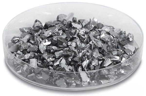
Forms commonly supplied include:
Silicon pieces or chunks
Granules
Pellets customized for evaporation crucibles
The material surface is cleaned and prepared to reduce oxide layers prior to packaging. During evaporation, stable melt behavior ensures consistent film thickness and uniform composition.
Typical resistivity ranges can be tailored depending on dopant concentration, supporting both lightly doped and highly conductive film requirements.
Applications
N-type Silicon Evaporation Materials are widely used in:
Thin film transistor (TFT) fabrication
Semiconductor device prototyping
Photovoltaic cell research
Microelectromechanical systems (MEMS)
Infrared detector structures
Integrated circuit development
Optoelectronic thin films
Layered heterostructure devices
In laboratory-scale semiconductor research, N-type Si films are often used as conductive layers, seed layers, or active semiconductor components.
Technical Parameters
| Parameter | Typical Value / Range | Importance |
|---|---|---|
| Material | N-type Silicon (Si) | Semiconductor functionality |
| Dopant Type | P / As / Sb (customizable) | Defines electrical properties |
| Purity | 99.999% (5N) or higher | Reduces contamination |
| Resistivity | 0.001 – 10 Ω·cm (customizable) | Controls conductivity |
| Form | Pieces / Granules / Pellets | Compatible with evaporation systems |
| Melting Point | 1414°C | Stable high-temperature behavior |
| Deposition Method | E-beam / Resistive Evaporation | Process flexibility |
Comparison with Related Materials
| Material | Key Advantage | Typical Application |
|---|---|---|
| N-type Silicon | Electron-rich semiconductor | Conductive thin films |
| P-type Silicon | Hole-rich semiconductor | Complementary device layers |
| Intrinsic Silicon | Very high resistivity | Insulating or buffer layers |
| Amorphous Silicon | Low-temperature deposition compatibility | Solar cells |
Compared with intrinsic silicon, N-type silicon provides significantly improved conductivity. Compared with P-type silicon, it offers complementary electrical behavior for junction formation in semiconductor devices.
FAQ
| Question | Answer |
|---|---|
| Can dopant concentration be customized? | Yes, resistivity and dopant levels can be tailored to meet specific device requirements. |
| Is the material suitable for electron beam evaporation? | Yes, it is optimized for stable melting in e-beam systems. |
| How is oxide formation controlled? | Materials are surface-cleaned and vacuum-sealed to minimize oxidation prior to use. |
| Can small research quantities be supplied? | Yes, flexible quantities are available for R&D purposes. |
| How is it packaged? | Vacuum-sealed, moisture-protected packaging ensures clean delivery. |
Packaging
Our N-type Silicon Evaporation Materials (Si) are meticulously tagged and labeled externally to ensure efficient identification and maintain high standards of quality control. We take great care to prevent contamination and mechanical damage during storage and transportation, ensuring the materials arrive in optimal condition.
Conclusion
N-type Silicon Evaporation Materials (Si) provide a reliable and high-purity solution for semiconductor thin film deposition and microelectronic device fabrication. With customizable dopant levels, controlled resistivity, and stable evaporation characteristics, they are well suited for advanced research and industrial applications.
For detailed specifications and a quotation, please contact us at sales@thinfilmmaterials.com.


Reviews
There are no reviews yet.