 MSDS File
Introduction
Cerium Gadolinium Evaporation Materials (Ce/Gd) are rare earth alloy sources engineered for precision thin film deposition in optical, electronic, magnetic, and functional coating systems. By combining cerium’s redox flexibility with gadolinium’s magnetic and neutron-absorbing characteristics, Ce/Gd alloys offer a versatile platform for advanced material research and specialized device fabrication.
In vacuum evaporation processes such as thermal and electron beam evaporation, alloy homogeneity and compositional stability directly influence film performance. Ce/Gd evaporation materials are produced with controlled composition and refined microstructure to ensure stable vaporization and consistent thin film properties across laboratory and industrial coating environments.
Detailed Description
Cerium (Ce) is known for its variable oxidation states (Ce³⁺/Ce⁴⁺), while Gadolinium (Gd) exhibits strong paramagnetic behavior and high magnetic moment. When alloyed, Ce/Gd materials enable tunable optical, electronic, and magnetic characteristics in deposited thin films.
Key features include:
Pre-Alloyed Composition Control – Accurate Ce/Gd ratios (wt% or at%) ensure reproducible film chemistry.
High Metal Purity (typically 3N–4N) – Low impurity levels minimize contamination in sensitive electronic or optical layers.
Dense Microstructure – Reduces particle generation and improves evaporation consistency.
Customizable Alloy Ratios – Tailored for specific magnetic, optical, or catalytic research applications.
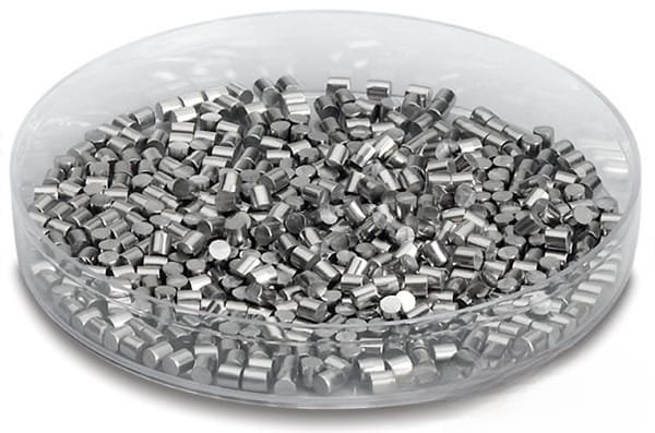
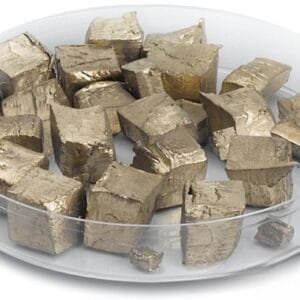
Ce/Gd evaporation materials are typically supplied in lump, granule, or pellet form compatible with tungsten boats, molybdenum crucibles, or graphite liners. Because rare earth metals are reactive, especially in finely divided form, handling in controlled environments and proper vacuum conditioning are recommended before deposition.
The alloy’s behavior during evaporation depends on composition and vapor pressure differences between Ce and Gd, so process optimization may be required to achieve precise stoichiometry in the deposited film.
Applications
Cerium Gadolinium Evaporation Materials are used in:
Magnetic Thin Film Research
Deposition of rare earth-containing layers for spintronic and magneto-optical studies.Optical & Functional Coatings
Films with tailored refractive index and optical absorption characteristics.Advanced Oxide Film Development
Ce/Gd precursor layers for post-oxidation to mixed rare earth oxides.Nuclear & Radiation-Related Research
Gd-containing films for neutron interaction studies (R&D scale).Thin Film Materials Science
Investigation of rare earth alloy phase behavior and electronic structure.
Technical Parameters
| Parameter | Typical Value / Range | Importance |
|---|---|---|
| Purity | 99.9% – 99.99% (3N–4N) | Reduces impurity-driven defects |
| Composition | Custom Ce/Gd ratio (wt% or at%) | Controls magnetic and optical properties |
| Form | Pieces / Granules / Pellets | Compatible with evaporation sources |
| Melting Point | Composition-dependent (~800–1300°C) | Affects evaporation strategy |
| Density | ≥ 99% theoretical (alloyed form) | Promotes stable vaporization |
| Packaging | Vacuum-sealed / inert atmosphere | Prevents oxidation |
Comparison with Related Rare Earth Materials
| Material | Key Advantage | Typical Application |
|---|---|---|
| Cerium Gadolinium (Ce/Gd) | Tunable magnetic & redox properties | Magnetic & functional films |
| Pure Cerium (Ce) | Strong redox behavior | Catalytic & oxide films |
| Pure Gadolinium (Gd) | High magnetic moment | Magneto-optical films |
| Gadolinium Oxide (Gd₂O₃) | Stable dielectric oxide | Electronic thin films |
Compared to single-element rare earth sources, Ce/Gd alloys offer synergistic functionality, enabling multi-property tuning within a single deposition material.
FAQ
| Question | Answer |
|---|---|
| Can the Ce/Gd ratio be customized? | Yes, alloy composition can be precisely adjusted according to experimental or production requirements. |
| Is the material supplied pre-alloyed? | Yes, standard products are pre-alloyed to ensure uniform evaporation behavior. |
| Are these materials reactive? | Rare earth metals are reactive and should be handled and stored in dry or inert conditions. |
| What evaporation methods are suitable? | Compatible with thermal and electron beam evaporation systems, depending on alloy composition. |
| Which industries use Ce/Gd films most? | Research institutions, magnetic materials laboratories, optics development, and advanced materials R&D. |
Packaging
Our Cerium Gadolinium Evaporation Materials are meticulously tagged and labeled externally to ensure efficient identification and maintain high standards of quality control. We take great care to prevent any potential damage during storage and transportation, ensuring the materials arrive in perfect condition.
Conclusion
Cerium Gadolinium Evaporation Materials (Ce/Gd) provide a flexible and high-purity solution for rare earth alloy thin film deposition. With customizable composition, controlled microstructure, and reliable vacuum packaging, Ce/Gd materials support advanced research and specialized industrial coating applications.
For detailed specifications and a quotation, please contact us at sales@thinfilmmaterials.com.


Reviews
There are no reviews yet.