Generic selectors
Exact matches only
Search in title
Search in content
Post Type Selectors

VD0537 Bismuth (Bi) Evaporation Materials

Material Type: Bismuth
Symbol: Bi
Color/Appearance: Lustrous Reddish White, Metallic
Purity: 99.9% ~ 99.999%
Shape: Powder/ Granule/ Custom-made

TFM provides bismuth evaporation materials and is a leading manufacturer and supplier of high-purity bismuth evaporating materials. We offer a wide range of evaporation materials in various forms, including powder, granules, and custom shapes tailored to your specific needs.

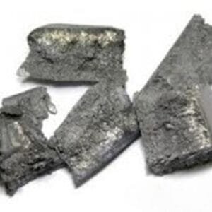
Bismuth Evaporation Materials Description

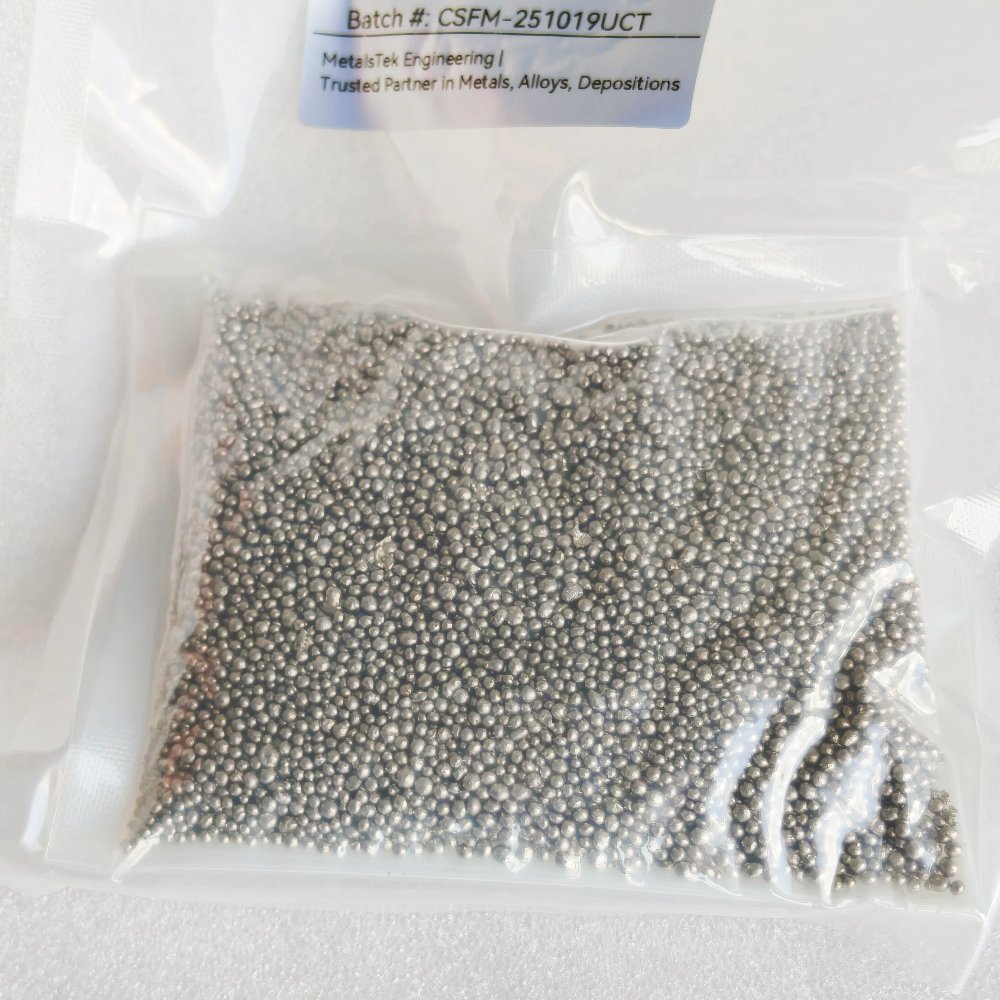
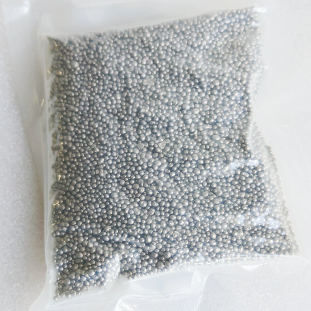
High-purity bismuth evaporation materials are crucial for achieving high-quality films in deposition processes. TFM specializes in producing bismuth evaporation materials with up to 99.999% purity, backed by stringent quality assurance processes to guarantee product reliability.

bismuth evaporation materials

Bismuth Evaporation Materials Specification

Material TypeBismuth
SymbolBi
Color/AppearanceLustrous Reddish White, Metallic
Melting Point2079 °C
Boiling Point1560 °C
Density9.747 g/cm3

Bismuth Evaporation Materials Applications

  • Deposition Processes: Employed in semiconductor deposition, chemical vapor deposition (CVD), and physical vapor deposition (PVD).
  • Optics: Used for wear protection, decorative coatings, and display technologies.

Bismuth Evaporation Materials Packaging

We handle our evaporation pellets with care to prevent any damage during storage and transportation, ensuring that their quality remains intact and preserved in their original condition.

Ordering Table 

Material Size Quantity Purity Part Number
Bismuth 3mm-6mm Pieces 25 g 99.999% EVMBI2-4MMA
Bismuth 3mm-6mm Pieces 50 g 99.999% EVMBI2-4MMB
Bismuth 3mm-6mm Pieces 100 g 99.999% EVMBI2-4MMD
Bismuth 3mm-6mm Pieces 200 g 99.999% EVMBI2-4MMH
Bismuth 3mm-6mm Pieces 250 g 99.999% EVMBI2-4MMJ
Bismuth 3mm-6mm Pieces 500 g 99.999% EVMBI2-4MMT

Reviews

There are no reviews yet.

Be the first to review “VD0537 Bismuth (Bi) Evaporation Materials”

Your email address will not be published. Required fields are marked *

FAQ

  • They are high‐purity substances (e.g. metals, alloys, or compounds) used in thermal or electron‐beam evaporation processes to form thin films on substrates.

  • Typically, they’re processed into a form (often ingots, pellets, or wires) that can be efficiently vaporized. Preparation emphasizes high purity and controlled composition to ensure film quality.

  • Thermal evaporation and electron-beam (e-beam) evaporation are the two main techniques, where material is heated (or bombarded with electrons) until it vaporizes and then condenses on the substrate.

  • Thermal evaporation heats the material directly (often using a resistive heater), while e-beam evaporation uses a focused electron beam to locally heat and vaporize the source material—each method offering different control and energy efficiency.

  • Key parameters include source temperature, vacuum level, deposition rate, substrate temperature, and the distance between the source and the substrate. These factors influence film uniformity, adhesion, and microstructure.

  • Evaporation generally produces high-purity films with excellent control over thickness, and it is especially suitable for materials with relatively low melting points or high vapor pressures.

  • Challenges include issues with step coverage (due to line-of-sight deposition), shadowing effects on complex topographies, and possible re-evaporation of material from the substrate if temperature isn’t properly controlled.

  • Common evaporation materials include noble metals (e.g., gold, silver), semiconductors (e.g., silicon, germanium), metal oxides, and organic compounds—each chosen for its specific optical, electrical, or mechanical properties.

  • Selection depends on desired film properties (conductivity, optical transparency, adhesion), compatibility with the evaporation process, and the final device application (semiconductor, optical coating, etc.).

  • Optimizing substrate temperature, deposition rate, and chamber vacuum are critical for ensuring that the film adheres well and forms the intended microstructure without defects.

  • Troubleshooting may involve checking the source material’s purity, ensuring stable source temperature, verifying the vacuum level, adjusting the substrate’s position or temperature, and monitoring deposition rate fluctuations.

While evaporation tends to yield very high purity films with excellent thickness control, it is limited by its line-of-sight nature. In contrast, sputtering can deposit films more uniformly on complex surfaces and is more versatile for a broader range of materials.


Shopping Cart
Scroll to Top