 MSDS File
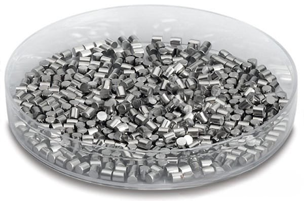
Cerium Samarium Evaporation Materials
TFM offers high-purity cerium samarium evaporation materials, which are alloys composed of cerium (Ce) and samarium (Sm). Our materials are produced with up to 99.9995% purity, ensuring superior performance in deposition processes. These high-quality materials are essential for producing top-tier deposited films and are manufactured with stringent quality assurance processes to guarantee reliability.
Applications
- Deposition Processes: Suitable for semiconductor deposition, chemical vapor deposition (CVD), and physical vapor deposition (PVD).
- Optics: Ideal for wear protection, decorative coatings, and display technologies.
Packaging and Handling
We take great care in handling and packaging our cerium samarium evaporation materials to avoid damage during storage and transportation, ensuring that they retain their high quality and arrive in optimal condition.
What We Offer
TFM is a leading manufacturer and supplier of high-purity cerium samarium evaporation materials, available in various forms such as powder and granules. Customized shapes and quantities can also be provided upon request. For current pricing and availability of these and other deposition materials not listed, please contact us with your inquiry.


Reviews
There are no reviews yet.