Generic selectors
Exact matches only
Search in title
Search in content
Post Type Selectors

VD0665 Zirconium Nickel Evaporation Materials, Zr/Ni

Catalog No.VD0665
MaterialZirconium Nickel (Zr/Ni)
Purity99.5%
ShapePowder/ Granule/ Custom-made

TFM stands out as a premier producer and distributor of high-purity zirconium and nickel evaporation materials, along with a diverse range of other evaporation materials. We provide these materials in both powder and granule forms, with the option for customized solutions to meet specific requirements.


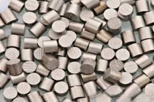
Zirconium Nickel Evaporation Materials Overview

TFM provides high-purity zirconium-nickel alloy evaporation materials, specifically designed for superior deposition processes. Our zirconium-nickel alloys are characterized by exceptional purity levels, reaching up to 99.9995%. This high purity is crucial for achieving top-quality thin films during various deposition processes. Our rigorous quality assurance procedures ensure the reliability of every product.

Applications of Zirconium Nickel Evaporation Materials

Zirconium-nickel evaporation materials are versatile and find applications in several fields:

  • Deposition Processes: Ideal for use in semiconductor deposition, chemical vapor deposition (CVD), and physical vapor deposition (PVD).
  • Optics: Employed in coatings for wear protection, decorative purposes, and display technologies.

Packaging and Handling

Our zirconium-nickel evaporation materials are meticulously tagged and labeled for easy identification and quality control. We prioritize careful packaging to prevent damage during storage and transportation.

Contact Us

TFM is a leading supplier of high-purity zirconium-nickel evaporation materials. We offer these materials in various forms, including tablets, granules, rods, and wires, with customization options available. Additionally, we supply evaporation sources, boats, filaments, crucibles, heaters, and e-beam crucible liners. For current pricing or to inquire about products not listed, please reach out to us.

Reviews

There are no reviews yet.

Be the first to review “VD0665 Zirconium Nickel Evaporation Materials, Zr/Ni”

Your email address will not be published. Required fields are marked *

FAQ

  • They are high‐purity substances (e.g. metals, alloys, or compounds) used in thermal or electron‐beam evaporation processes to form thin films on substrates.

  • Typically, they’re processed into a form (often ingots, pellets, or wires) that can be efficiently vaporized. Preparation emphasizes high purity and controlled composition to ensure film quality.

  • Thermal evaporation and electron-beam (e-beam) evaporation are the two main techniques, where material is heated (or bombarded with electrons) until it vaporizes and then condenses on the substrate.

  • Thermal evaporation heats the material directly (often using a resistive heater), while e-beam evaporation uses a focused electron beam to locally heat and vaporize the source material—each method offering different control and energy efficiency.

  • Key parameters include source temperature, vacuum level, deposition rate, substrate temperature, and the distance between the source and the substrate. These factors influence film uniformity, adhesion, and microstructure.

  • Evaporation generally produces high-purity films with excellent control over thickness, and it is especially suitable for materials with relatively low melting points or high vapor pressures.

  • Challenges include issues with step coverage (due to line-of-sight deposition), shadowing effects on complex topographies, and possible re-evaporation of material from the substrate if temperature isn’t properly controlled.

  • Common evaporation materials include noble metals (e.g., gold, silver), semiconductors (e.g., silicon, germanium), metal oxides, and organic compounds—each chosen for its specific optical, electrical, or mechanical properties.

  • Selection depends on desired film properties (conductivity, optical transparency, adhesion), compatibility with the evaporation process, and the final device application (semiconductor, optical coating, etc.).

  • Optimizing substrate temperature, deposition rate, and chamber vacuum are critical for ensuring that the film adheres well and forms the intended microstructure without defects.

  • Troubleshooting may involve checking the source material’s purity, ensuring stable source temperature, verifying the vacuum level, adjusting the substrate’s position or temperature, and monitoring deposition rate fluctuations.

While evaporation tends to yield very high purity films with excellent thickness control, it is limited by its line-of-sight nature. In contrast, sputtering can deposit films more uniformly on complex surfaces and is more versatile for a broader range of materials.


Shopping Cart
Scroll to Top