Introduction
Zinc Oxide doped with Gallium Oxide Evaporation Materials (ZnO/Ga₂O₃) are widely used in thin film deposition processes to produce transparent conductive oxide (TCO) coatings. Gallium-doped zinc oxide (commonly referred to as GZO) combines the excellent optical transparency of ZnO with enhanced electrical conductivity provided by gallium doping. These materials are commonly used in optoelectronic devices, display technologies, photovoltaic cells, and transparent electronics.
When used in thermal evaporation or electron beam evaporation systems, ZnO/Ga₂O₃ evaporation materials enable the deposition of uniform conductive oxide films with high transparency in the visible spectrum and good electrical conductivity, making them an important alternative to indium-based conductive materials.
Detailed Description
ZnO/Ga₂O₃ evaporation materials are produced by carefully mixing high-purity zinc oxide and gallium oxide powders followed by controlled sintering or solid-state reaction processes. These manufacturing techniques ensure homogeneous doping distribution and stable material composition, which are essential for achieving consistent film properties during evaporation deposition.
Gallium acts as an effective n-type dopant in zinc oxide by substituting zinc atoms in the ZnO crystal lattice. This substitution introduces additional free electrons into the material, significantly improving electrical conductivity while maintaining excellent optical transparency. Compared with other dopants such as aluminum or indium, gallium offers strong thermal stability and improved resistance to oxidation and diffusion.
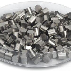
The resulting evaporation materials are typically supplied in granules, pellets, tablets, or pieces optimized for use in electron beam evaporation, resistive heating evaporation, or other physical vapor deposition systems. The uniformity of the material ensures stable evaporation rates and consistent film composition.
ZnO/Ga₂O₃ thin films deposited from these materials exhibit excellent optical transparency, good electrical conductivity, and high chemical stability. These properties make them highly suitable for transparent electrode layers and functional oxide coatings in modern optoelectronic technologies.
Applications
ZnO/Ga₂O₃ evaporation materials are widely used in several advanced technology sectors:
Transparent conductive oxide (TCO) films for display panels and touch screens
Thin film solar cells as transparent electrode layers
Optoelectronic devices such as LEDs and photodetectors
Transparent electronics and smart glass technologies
Optical coatings requiring high transparency and electrical conductivity
Research and development of next-generation oxide semiconductors
Technical Parameters
| Parameter | Typical Value / Range | Importance |
|---|---|---|
| Purity | 99.9% – 99.99% | High purity improves optical and electrical film performance |
| Composition | ZnO with Ga₂O₃ doping (typically 1–5 wt%) | Controls electrical conductivity and carrier concentration |
| Form | Pellets / Granules / Tablets | Compatible with evaporation sources |
| Particle Size | 1 – 6 mm typical | Ensures stable evaporation behavior |
| Density | High density sintered material | Provides consistent evaporation rates |
| Deposition Method | E-beam evaporation / Thermal evaporation | Suitable for PVD thin film deposition |
Comparison with Related Materials
| Material | Key Advantage | Typical Application |
|---|---|---|
| ZnO/Ga₂O₃ (GZO) | Transparent conductive oxide with good thermal stability | Displays, solar cells, and optoelectronics |
| Aluminum-doped ZnO (AZO) | Cost-effective TCO material | Solar cells and transparent electrodes |
| Indium Tin Oxide (ITO) | Very high conductivity and transparency | Displays and touch panels |
FAQ
| Question | Answer |
|---|---|
| What forms are available for ZnO/Ga₂O₃ evaporation materials? | They are typically supplied as pellets, granules, tablets, or pieces suitable for evaporation sources. |
| What deposition methods are compatible with this material? | ZnO/Ga₂O₃ materials are commonly used in electron beam evaporation and thermal evaporation systems. |
| What is the typical gallium doping concentration? | Gallium oxide doping typically ranges from 1% to 5%, depending on the desired conductivity and optical properties. |
| What substrates can GZO films be deposited on? | GZO films can be deposited on glass, silicon wafers, flexible polymers, and ceramic substrates. |
| Why use GZO instead of ITO? | GZO provides a more cost-stable alternative since it avoids the use of indium while maintaining good transparency and conductivity. |
Packaging
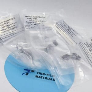
Our Zinc Oxide doped with Gallium Oxide Evaporation Materials (ZnO/Ga₂O₃) are meticulously tagged and labeled externally to ensure efficient identification and maintain high standards of quality control. The materials are packaged in vacuum-sealed bags or inert atmosphere containers with protective packaging to prevent contamination or moisture exposure during storage and transportation.
Conclusion
ZnO/Ga₂O₃ evaporation materials provide a reliable solution for depositing transparent conductive oxide films used in modern optoelectronic devices. By combining zinc oxide’s optical transparency with gallium’s effective n-type doping, these materials enable high-performance thin films suitable for solar cells, displays, and transparent electronics.
With customizable compositions, high-purity raw materials, and consistent evaporation performance, ZnO/Ga₂O₃ evaporation materials support advanced thin film technologies and next-generation optoelectronic applications.
For detailed specifications and a quotation, please contact us at sales@thinfilmmaterials.com.


 MSDS File


Reviews
There are no reviews yet.