
 MSDS File
Introduction
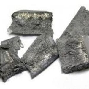
Iron(II) Sulfide evaporation materials are important metal sulfide compounds used in thin-film deposition for semiconductor research, energy materials, and functional coatings. With its distinctive electronic and chemical characteristics, Iron(II) Sulfide (FeS) serves as a valuable source material for depositing sulfide-based thin films via vacuum evaporation processes, supporting both fundamental research and emerging device development.
Detailed Description
Iron(II) Sulfide is a binary metal sulfide composed of iron and sulfur, typically exhibiting semiconducting behavior and strong chemical reactivity toward chalcogen-based systems. In thin-film form, FeS has attracted interest for applications related to energy conversion, catalysis, and electronic materials research.
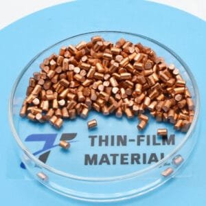
Our Iron(II) Sulfide evaporation materials are synthesized from high-purity iron and sulfur under carefully controlled conditions to achieve consistent stoichiometry and phase stability. The material is processed into pellets, granules, or custom geometries suitable for thermal evaporation and electron-beam evaporation systems. Dense, uniform material structure helps ensure stable evaporation rates and reduces spitting or composition fluctuation during deposition.
Due to the sulfur content, special attention is given to material handling and packaging to minimize oxidation and moisture exposure. When properly evaporated under controlled vacuum conditions, Iron(II) Sulfide enables reproducible thin-film growth with reliable chemical composition.
Applications
Iron(II) Sulfide evaporation materials are commonly used in:
Semiconductor and chalcogenide thin-film research
Energy-related materials and conversion studies
Catalytic and electrochemical thin films
Functional sulfide coatings
Laboratory-scale thin-film deposition and R&D
Technical Parameters
| Parameter | Typical Value / Range | Importance |
|---|---|---|
| Material | Iron(II) Sulfide (FeS) | Defines chemical & electronic behavior |
| Purity | 99.9% – 99.99% | Minimizes contamination in thin films |
| Form | Pellet / Granule / Custom | Ensures controlled evaporation |
| Pellet Size | 1 – 6 mm (custom available) | Fits common crucibles |
| Deposition Method | Thermal / E-beam evaporation | Compatible with standard PVD systems |
| Sensitivity | Moisture & oxidation sensitive | Requires controlled handling |
Comparison with Related Materials
| Material | Key Advantage | Typical Application |
|---|---|---|
| Iron(II) Sulfide (FeS) | Simple metal sulfide chemistry | Sulfide thin-film research |
| Iron Disulfide (FeS₂) | Narrow bandgap, photovoltaic interest | Energy materials |
| Zinc Sulfide (ZnS) | Wide bandgap | Optical coatings |
| Copper Sulfide (Cu₂S) | High conductivity | Semiconductor films |
FAQ
| Question | Answer |
|---|---|
| Is Iron(II) Sulfide suitable for thermal evaporation? | Yes, it is commonly used in thermal and e-beam evaporation systems. |
| Can material form be customized? | Yes, pellets, granules, and custom shapes are available. |
| How is sulfur loss controlled during evaporation? | Optimized material density and controlled deposition conditions help maintain composition. |
| How is the material packaged? | Vacuum-sealed or inert-gas packed to prevent oxidation and moisture exposure. |
Packaging
Our Iron(II) Sulfide Evaporation Materials are meticulously tagged and labeled externally to ensure efficient identification and strict quality control. Each batch is vacuum-sealed or packed under inert atmosphere and protected with shock-absorbing materials to preserve material integrity during storage and transportation.
Conclusion
Iron(II) Sulfide evaporation materials provide a reliable and high-purity source for depositing sulfide-based thin films in research and advanced material development. With controlled composition, stable evaporation behavior, and flexible form options, FeS is a dependable choice for semiconductor, energy, and functional coating studies.
For detailed specifications and a quotation, please contact us at sales@thinfilmmaterials.com.

Reviews
There are no reviews yet.