 MSDS File
Introduction
Tantalum Boride (TaB₂) Evaporation Materials are ultra-high-temperature ceramic sources designed for depositing hard, conductive boride thin films in physical vapor deposition (PVD) systems. TaB₂ is known for its exceptional hardness, high melting point (above 3000 °C), excellent chemical stability, and relatively good electrical conductivity among ceramics. These properties make it highly suitable for protective coatings, diffusion barriers, and high-temperature functional layers.
Detailed Description
Our Tantalum Boride Evaporation Materials are produced from high-purity tantalum and boron under tightly controlled synthesis conditions to ensure accurate stoichiometry and phase stability. Maintaining the precise Ta:B ratio is essential, as deviations can affect film hardness, oxidation resistance, and electrical behavior.
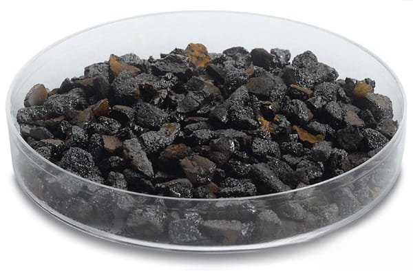
TaB₂ is supplied in forms suitable for electron-beam evaporation and, in certain configurations, high-temperature thermal evaporation. Typical forms include granules, pellets, and custom-cut pieces to match various crucibles and evaporation sources. Controlled particle sizing ensures stable heating behavior and minimizes spitting during high-energy evaporation.
Due to its very high melting point and refractory nature, electron-beam evaporation is generally recommended for stable deposition. Strict impurity control—especially oxygen and metallic contaminants—is critical to achieving high-performance thin films with reliable mechanical and chemical properties.
Applications
Tantalum Boride Evaporation Materials are widely used in advanced coating and materials research applications, including:
Hard, wear-resistant protective coatings
High-temperature and oxidation-resistant films
Diffusion barrier layers in microelectronics
Aerospace and plasma-facing components research
Conductive ceramic coatings
Advanced boride thin film R&D
Technical Parameters
| Parameter | Typical Value / Range | Importance |
|---|---|---|
| Chemical Composition | TaB₂ | Determines hardness & thermal stability |
| Purity | 99.5% – 99.9% | Reduces impurity-related film defects |
| Form | Pellets / Granules / Custom | Compatible with evaporation sources |
| Particle Size | 1 – 6 mm (custom available) | Ensures stable evaporation |
| Melting Point | ~3040 °C | Suitable for extreme environments |
| Evaporation Method | E-beam (recommended) | Ensures stable high-temperature evaporation |
Comparison with Related Boride Materials
| Material | Key Advantage | Typical Application |
|---|---|---|
| TaB₂ | High hardness & oxidation resistance | Protective coatings |
| TiB₂ | Excellent conductivity | Wear-resistant films |
| ZrB₂ | Ultra-high-temperature stability | Thermal protection |
| HfB₂ | Extreme oxidation resistance | Aerospace coatings |
FAQ
| Question | Answer |
|---|---|
| Which evaporation method is recommended for TaB₂? | Electron-beam evaporation is generally recommended due to its high melting point. |
| Can particle size be customized? | Yes, granule and pellet sizes can be tailored to your system requirements. |
| Is TaB₂ electrically conductive? | Yes, it has relatively good conductivity for a ceramic material. |
| How is the material packaged? | Vacuum-sealed or inert-gas packed to prevent contamination and moisture exposure. |
Packaging
Our Tantalum Boride (TaB₂) Evaporation Materials are meticulously tagged and labeled externally to ensure efficient identification and maintain high standards of quality control. We take great care to prevent contamination or mechanical damage during storage and transportation, ensuring the materials arrive in optimal condition.
Conclusion
Tantalum Boride (TaB₂) Evaporation Materials provide a robust solution for depositing ultra-hard, high-temperature boride thin films with excellent chemical and thermal stability. With controlled stoichiometry, high purity, and customizable forms, TaB₂ is well suited for aerospace, electronics, and advanced protective coating applications.
For detailed specifications and a quotation, please contact us at sales@thinfilmmaterials.com.


Reviews
There are no reviews yet.