Generic selectors
Exact matches only
Search in title
Search in content
Post Type Selectors

VD0868 Tantalum Telluride Evaporation Materials, TaTe2

Catalog No.VD0868
MaterialTantalum Telluride (TaTe2)
Purity99.9% ~ 99.999%
ShapePowder/ Granule/ Custom-made

TFM stands out as a top-tier manufacturer and supplier specializing in high-purity tantalum telluride evaporation materials. Our extensive range of evaporation materials is available in both powder and granule forms to meet diverse needs. For clients requiring tailored solutions, we also offer customized forms upon request.

Tantalum Telluride Evaporation Materials Overview

Tantalum telluride evaporation materials, identified by the chemical formula TaTe2, are crucial in various deposition processes. TFM specializes in crafting these materials with exceptional purity levels, reaching up to 99.9995%. Our stringent quality assurance procedures ensure that our tantalum telluride materials contribute to the production of high-quality films.

Tantalum Telluride Evaporation Materials Specifications

  • Material Type: Tantalum Telluride
  • Chemical Symbol: TaTe2
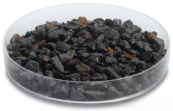
  • Appearance: Crystalline solid
  • Density: 9.4 g/cm³
  • Purity: 99.9% – 99.999%
  • Form: Powder/Granule/Custom-made

Applications of Tantalum Telluride Evaporation Materials

Our tantalum telluride evaporation materials are utilized in a variety of deposition techniques, including:

  • Semiconductor Deposition
  • Chemical Vapor Deposition (CVD)
  • Physical Vapor Deposition (PVD)

These materials are ideal for applications in optics, such as wear protection, decorative coatings, and display technologies.

Packaging and Quality Assurance

To maintain the highest quality, our tantalum telluride evaporation materials are securely packaged in plastic vacuum bags. This packaging protects the materials from damage and preserves their quality during storage and transportation. Each shipment also includes a Certificate of Analysis (COA) to confirm the purity and reliability of the product.

Contact Us

TFM is committed to delivering premium tantalum telluride evaporation materials for various applications, from semiconductors to optical coatings. Our expertise in engineering, manufacturing, and analysis ensures we provide top-quality products. For inquiries or quotes, please get in touch with us today.

Reviews

There are no reviews yet.

Be the first to review “VD0868 Tantalum Telluride Evaporation Materials, TaTe2”

Your email address will not be published. Required fields are marked *

FAQ

  • They are high‐purity substances (e.g. metals, alloys, or compounds) used in thermal or electron‐beam evaporation processes to form thin films on substrates.

  • Typically, they’re processed into a form (often ingots, pellets, or wires) that can be efficiently vaporized. Preparation emphasizes high purity and controlled composition to ensure film quality.

  • Thermal evaporation and electron-beam (e-beam) evaporation are the two main techniques, where material is heated (or bombarded with electrons) until it vaporizes and then condenses on the substrate.

  • Thermal evaporation heats the material directly (often using a resistive heater), while e-beam evaporation uses a focused electron beam to locally heat and vaporize the source material—each method offering different control and energy efficiency.

  • Key parameters include source temperature, vacuum level, deposition rate, substrate temperature, and the distance between the source and the substrate. These factors influence film uniformity, adhesion, and microstructure.

  • Evaporation generally produces high-purity films with excellent control over thickness, and it is especially suitable for materials with relatively low melting points or high vapor pressures.

  • Challenges include issues with step coverage (due to line-of-sight deposition), shadowing effects on complex topographies, and possible re-evaporation of material from the substrate if temperature isn’t properly controlled.

  • Common evaporation materials include noble metals (e.g., gold, silver), semiconductors (e.g., silicon, germanium), metal oxides, and organic compounds—each chosen for its specific optical, electrical, or mechanical properties.

  • Selection depends on desired film properties (conductivity, optical transparency, adhesion), compatibility with the evaporation process, and the final device application (semiconductor, optical coating, etc.).

  • Optimizing substrate temperature, deposition rate, and chamber vacuum are critical for ensuring that the film adheres well and forms the intended microstructure without defects.

  • Troubleshooting may involve checking the source material’s purity, ensuring stable source temperature, verifying the vacuum level, adjusting the substrate’s position or temperature, and monitoring deposition rate fluctuations.

While evaporation tends to yield very high purity films with excellent thickness control, it is limited by its line-of-sight nature. In contrast, sputtering can deposit films more uniformly on complex surfaces and is more versatile for a broader range of materials.


Shopping Cart
Scroll to Top