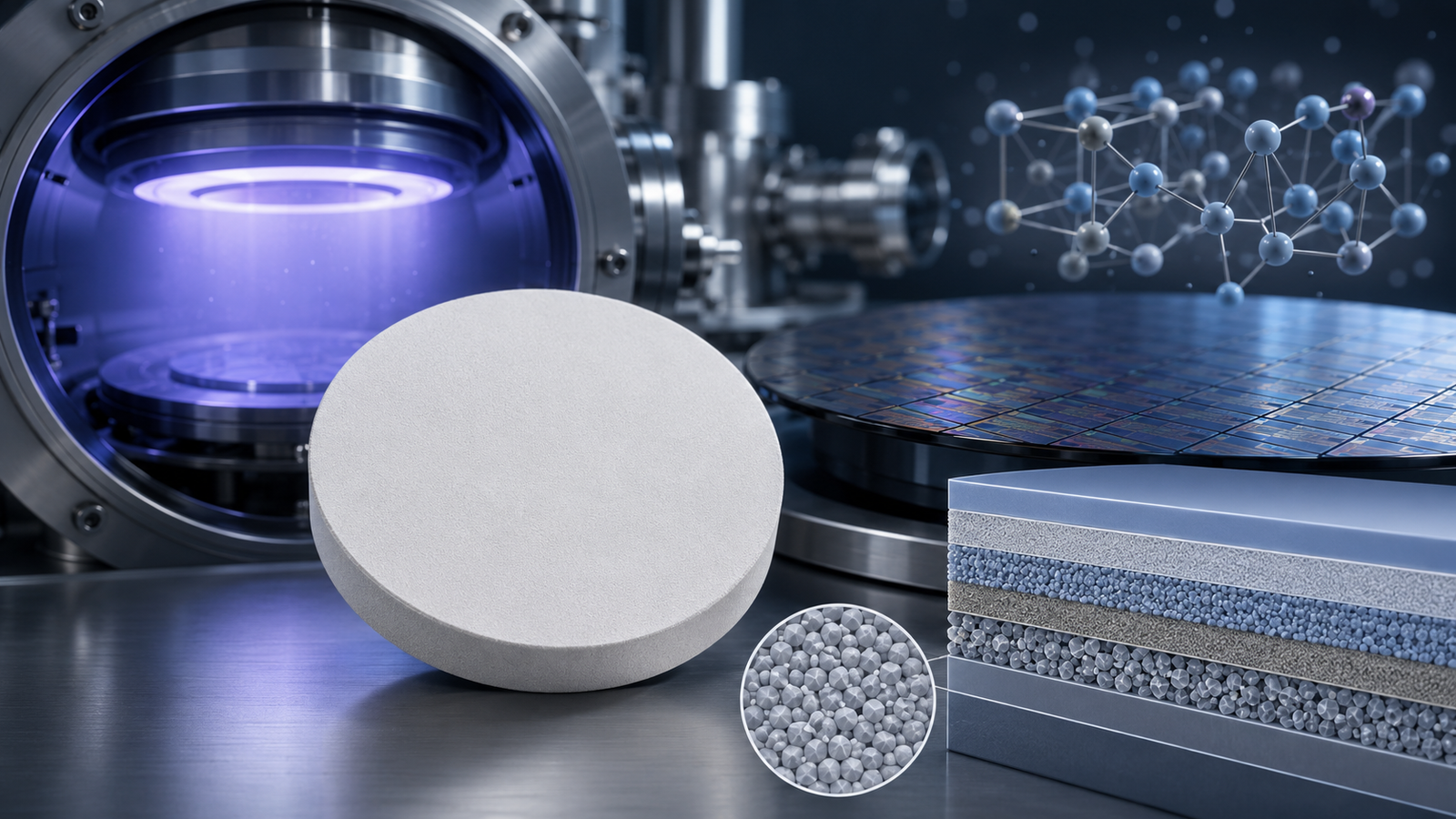
The process of sputtering deposition is fundamental to various industries, including semiconductor manufacturing, thin-film coatings, and advanced materials science. Sputtering, an essential part of the vacuum deposition family, involves bombarding a target material with energetic ions, typically from a plasma, to eject atoms from the target surface. These atoms are then deposited onto a substrate, forming a thin film. The efficiency, quality, and consistency of sputtering deposition rely heavily on the quality of the sputtering targets used. Over the years, significant advancements have been made in sputtering target technology, offering new opportunities for improving deposition performance, enhancing film characteristics, and optimizing industrial processes.
This article delves into the role of cutting-edge sputtering targets in enhancing sputtering deposition performance. We will explore how advanced sputtering targets contribute to superior film quality, higher uniformity, better control, and increased efficiency, while also highlighting their impact on various industries and applications.
The Fundamentals of Sputtering Deposition
Sputtering is a physical vapor deposition (PVD) technique where atoms or molecules are ejected from a solid target material by energetic ions. These atoms then travel through a vacuum or low-pressure gas environment and condense onto a substrate, forming a thin film. This technique is widely used for depositing materials onto substrates in semiconductor devices, solar cells, optics, and coatings.
The sputtering process consists of several steps:
- Ionization of Gas: In the sputtering chamber, a noble gas (such as argon) is ionized by an electrical field to form a plasma.
- Acceleration of Ions: The ions are accelerated towards the target material.
- Sputtering of Target Material: When ions collide with the target, they transfer energy to the target atoms, ejecting them from the surface.
- Deposition of Atoms: The ejected atoms travel toward the substrate and condense to form a thin film.
The overall quality of the deposited film is influenced by many factors, including the properties of the sputtering target, the sputtering process parameters (such as power, pressure, and gas composition), and the substrate characteristics.
The Role of Sputtering Targets in Deposition Performance
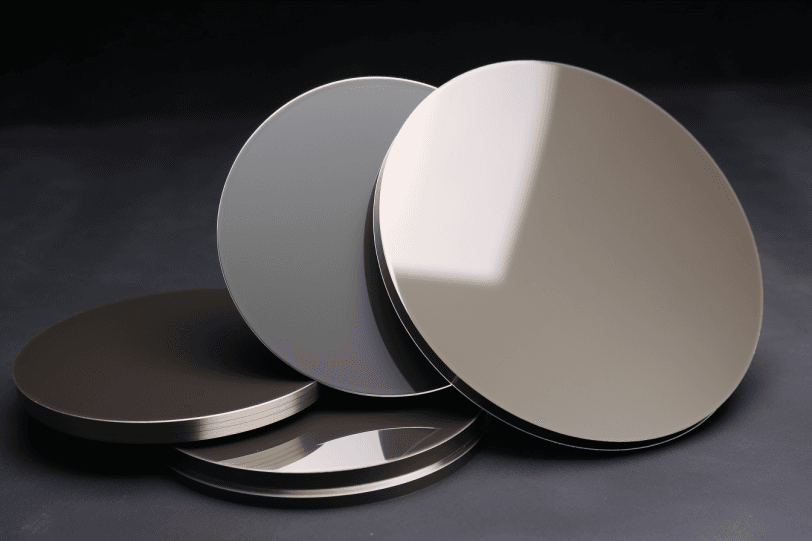
Sputtering targets are typically made of metals, alloys, oxides, or other materials, depending on the desired film properties. The target material plays a critical role in determining the characteristics of the deposited film, such as its composition, texture, adhesion strength, and electrical and optical properties. As the demand for more precise, uniform, and high-performance thin films grows, the role of advanced sputtering targets has become even more crucial.
Cutting-edge sputtering targets are designed to optimize various aspects of the sputtering process. They allow manufacturers to achieve better material utilization, higher film quality, increased process stability, and reduced contamination. These advancements not only improve the final product but also contribute to more efficient and cost-effective production processes.
High-Purity Materials for Superior Film Quality
One of the primary factors influencing sputtering performance is the purity of the target material. High-purity sputtering targets are critical for achieving high-quality thin films. Contamination from impurities in the target material can adversely affect the film’s properties, leading to defects such as poor adhesion, irregular surface morphology, and undesirable electrical or optical characteristics. As the demand for advanced, high-performance devices in industries like semiconductors, data storage, and solar energy increases, the need for ultra-pure sputtering targets has become even more pronounced.
Modern sputtering targets are manufactured from high-purity metals, alloys, and compounds to ensure minimal contamination during the sputtering process. For example, targets made from pure metals like copper, gold, platinum, and aluminum are widely used in industries such as microelectronics and optics, where the quality of the thin film directly impacts device performance. High-purity targets are also essential for creating thin films with consistent composition and precise physical properties, such as resistivity, refractive index, and conductivity.
Target Material Customization for Specific Applications
Cutting-edge sputtering targets offer customization options to meet the unique requirements of different industries and applications. Advances in material science and manufacturing techniques enable the production of sputtering targets that are tailored to specific performance criteria. These include customized alloy compositions, sizes, geometries, and surface finishes. Custom targets can be engineered to optimize film properties such as hardness, corrosion resistance, optical transmittance, or magnetic permeability.
For instance, in semiconductor manufacturing, sputtering targets can be tailored to create films with specific electrical properties for integrated circuits, transistors, and photonic devices. Similarly, in the automotive and aerospace industries, sputtering targets made from specialized alloys can be used to produce thin films with enhanced wear resistance or low friction properties for high-performance components.
Customization also extends to the choice of reactive sputtering targets, which are used to deposit compound films like oxides, nitrides, and carbides. By adjusting the composition of the sputtering target, manufacturers can control the stoichiometry of the deposited film and achieve specific material characteristics that would be difficult to obtain using pure metals alone.
Enhanced Uniformity and Thickness Control
The uniformity of a thin film is critical in applications such as semiconductor fabrication, optics, and data storage. Non-uniformities in film thickness can result in performance issues, including poor electrical conductivity, uneven surface properties, or optical distortions. Cutting-edge sputtering targets are designed to ensure high film uniformity, providing consistent coverage across the substrate.
One of the key advancements in sputtering target technology is the ability to maintain a more uniform erosion profile throughout the life of the target. Traditional sputtering targets tend to erode unevenly over time, which can lead to variations in film thickness and composition. Modern sputtering targets, however, are engineered to exhibit more consistent erosion patterns, ensuring that the deposition process remains stable throughout the target’s lifetime.
Additionally, advanced sputtering targets can improve thickness control by offering better material utilization. With precise engineering, manufacturers can minimize material loss during sputtering, which not only improves deposition efficiency but also contributes to more consistent film thickness. For applications requiring extremely precise film thickness, such as in optical coatings or multilayered devices, the use of advanced sputtering targets becomes essential.
Longer Target Lifespan and Reduced Downtime
In many industrial applications, reducing downtime is critical to improving throughput and maintaining operational efficiency. Sputtering targets that are designed for durability can significantly extend the lifespan of the target, reducing the frequency of replacements and minimizing the need for maintenance.
Advanced sputtering targets are made from materials with higher resistance to wear, corrosion, and contamination. These targets are engineered to provide consistent performance over longer periods, allowing manufacturers to achieve more stable deposition rates and better overall process control. Longer-lasting targets also contribute to reduced material costs, as less frequent replacements are required.
In addition to improving target durability, cutting-edge sputtering targets are also designed to reduce issues such as target poisoning. Target poisoning occurs when reactive gases, such as oxygen or nitrogen, interact with the target material during sputtering, leading to the formation of a contaminant layer on the target surface. This can significantly reduce the efficiency of the sputtering process and affect the quality of the deposited film. Modern sputtering targets are designed with materials and coatings that are more resistant to poisoning, ensuring that the deposition process remains stable and efficient.
Reduced Target Poisoning and Contamination
Target poisoning is a significant challenge in reactive sputtering processes, where gases like oxygen, nitrogen, or carbon are introduced into the chamber to form compound films. The reactive gases can interact with the target material, forming oxides, nitrides, or carbides that build up on the target surface, leading to performance degradation. Over time, this can result in uneven film composition, poor film quality, and the need for frequent target replacements.
Cutting-edge sputtering targets are designed to resist target poisoning and minimize contamination. This is achieved through the use of advanced materials that are less reactive with the gases used in the sputtering process. For example, certain alloys or composite materials may be employed to provide a more stable surface, reducing the formation of unwanted compounds. Additionally, improved target surface coatings can prevent the target from reacting with reactive gases, thereby ensuring more consistent film quality.
Applications of Advanced Sputtering Targets
Cutting-edge sputtering targets are used in a wide range of industries and applications, where their enhanced performance contributes to the production of high-quality thin films. Some of the most prominent applications include:
1. Semiconductor Manufacturing
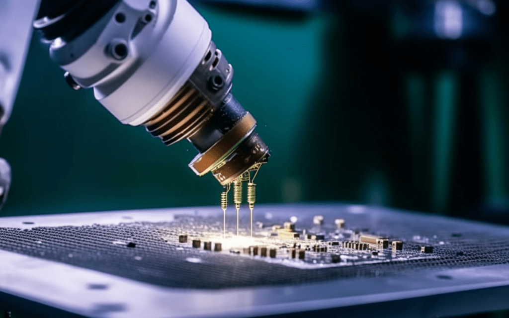
Sputtering deposition is a key technique in semiconductor manufacturing, where it is used to deposit thin films for integrated circuits (ICs), transistors, photonic devices, and other microelectronic components. The need for high-quality, uniform films with precise electrical properties makes sputtering an ideal method for these applications. Advanced sputtering targets enable semiconductor manufacturers to achieve the high purity, film uniformity, and specific electrical characteristics required for the production of cutting-edge devices.
2. Solar Energy
In the solar energy industry, sputtering deposition is used to create thin-film solar cells, including copper indium gallium selenide (CIGS) and cadmium telluride (CdTe) solar cells. These thin-film technologies offer advantages over traditional silicon-based solar cells, including lower manufacturing costs and greater flexibility. Advanced sputtering targets are used to deposit the various layers of the thin-film solar cells, providing better material utilization, higher film quality, and more consistent performance across large-area substrates.
3. Data Storage
Sputtering targets are used to produce magnetic thin films for data storage devices, such as hard disk drives (HDDs) and magnetic random-access memory (MRAM). The precise control over the magnetic properties of the thin films is crucial for the performance and reliability of these devices. Advanced sputtering targets enable manufacturers to deposit high-quality magnetic films with specific characteristics, such as high coercivity, low noise, and excellent thermal stability.
4. Optical Coatings
Sputtering is widely used in the production of optical coatings, including antireflection coatings, mirrors, filters, and lenses. The quality of the thin films deposited for optical applications must meet stringent specifications for optical transmittance, reflectance, and uniformity. Cutting-edge sputtering targets allow for the deposition of high-performance optical coatings with precise control over the film’s refractive index, thickness, and surface morphology.
5. Wear-Resistant Coatings
Sputtering deposition is also employed to apply wear-resistant coatings to tools, automotive components, medical devices, and other industrial applications. These coatings improve the durability and performance of components exposed to harsh environments. Advanced sputtering targets, often made from hard materials like titanium, tungsten, and zirconium, provide superior wear resistance, corrosion resistance, and hardness.
Conclusion
The development of cutting-edge sputtering targets has significantly enhanced sputtering deposition performance across a wide range of industries. With advancements in material science and manufacturing processes, these targets enable higher film quality, greater uniformity, better control over film properties, and improved efficiency in sputtering processes. The use of high-purity materials, customized target compositions, and improved durability has led to the creation of more reliable, cost-effective sputtering processes for applications in semiconductor manufacturing, solar energy, data storage, optics, and more.
As industries continue to demand more precise, high-performance thin films, the role of advanced sputtering targets will become increasingly important in achieving these goals. By investing in cutting-edge sputtering targets, manufacturers can improve the quality of their thin films, increase process efficiency, and stay competitive in an ever-evolving technological landscape.