Project Background
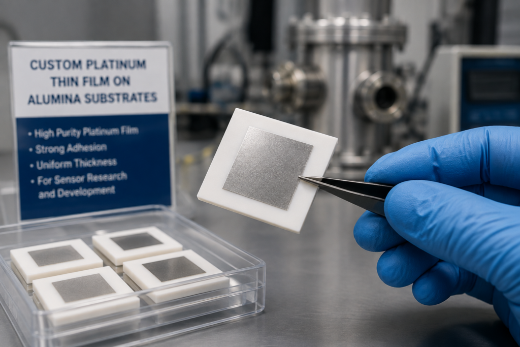
A research customer needed a small batch of custom platinum thin film on alumina substrates for sensor development. The project was not a standard catalog purchase because the requirement involved both the substrate and the functional metal film. The customer required an electrically stable platinum layer on an insulating ceramic base, with controlled coating thickness, good adhesion, clean handling, and consistent appearance across the batch.
For sensor research, the substrate is not just a mechanical support. It affects film adhesion, thermal behavior, electrical isolation, surface cleanliness, and long-term repeatability. Alumina was selected because it is a widely used oxide ceramic substrate with good mechanical stability and electrical insulation. NIST’s ceramics database classifies alumina as an oxide ceramic material and records structural ceramic property data for Al₂O₃, making it a common reference material in engineering and research contexts.
Platinum was selected as the thin-film material because the device required a noble metal layer with reliable electrical behavior, chemical stability, and compatibility with sensor testing environments. Platinum is also widely used in thin-film metallization, electrodes, temperature-sensing structures, and microfabrication research. NIST provides atomic reference data for platinum, including its elemental identity and atomic data, which is useful for material identification and technical documentation.
The project goal was simple in concept but demanding in execution:
Deposit a uniform platinum thin film onto alumina ceramic substrates and supply coated samples that were clean, traceable, and ready for laboratory evaluation.
Suggested external keyword links for publication:
Customer Requirement
The customer’s application involved sensor research, where the platinum-coated ceramic substrate would be used as a functional test platform. The substrate needed to provide insulation and dimensional stability, while the platinum film needed to provide a conductive and chemically stable surface.
A typical requirement for this type of project may include:
| Item | Project Requirement |
|---|---|
| Substrate | Alumina ceramic substrate |
| Coating Material | Platinum thin film |
| Optional Adhesion Layer | Ti, Cr, or other reviewed interlayer |
| Coating Area | Full-area coating or defined coating region |
| Film Thickness | Customer-specified nanometer-scale thickness |
| Surface Condition | Clean, uniform, free from obvious peeling or contamination |
| Application | Sensor research, electrode testing, or functional thin-film evaluation |
| Documentation | Material identification, coating specification, batch record, packaging record |
The exact film thickness, adhesion layer, and coating area were reviewed according to the customer’s drawing and device concept.
Unlike a simple substrate order, this project required coordination between several technical details:
- Ceramic substrate selection
- Surface cleaning before deposition
- Platinum deposition route
- Adhesion-layer evaluation
- Film thickness control
- Handling and packaging
- Batch-to-batch repeatability
For thin-film sensor components, even small changes in substrate surface condition or coating process can affect adhesion, resistance, and device test results.
Why Alumina Was Selected as the Substrate
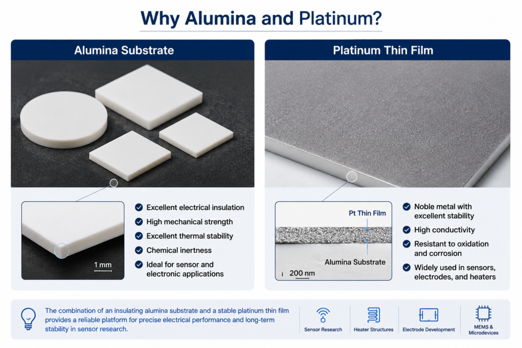
Alumina is one of the most commonly used ceramic substrates in sensor and electronic applications. It provides a practical balance of insulation, mechanical strength, thermal stability, and process compatibility.
For this project, alumina offered several advantages.
First, alumina is electrically insulating, which is important when the platinum film functions as a patterned electrode, heater layer, or sensor-related conductive surface. The substrate must not short the circuit or interfere with measurement.
Second, alumina is mechanically stable. Thin ceramic substrates can be handled, cleaned, coated, and packaged with reasonable reliability when the dimensions and surface condition are properly specified.
Third, alumina is compatible with many thin-film metallization processes. It is often used as a platform for noble metal films, resistor films, heater structures, and sensor electrodes.
However, alumina also introduces process challenges. Ceramic substrates may have surface roughness, porosity, edge chips, or adsorbed contaminants. These factors can influence platinum film nucleation and adhesion. A successful coated substrate project therefore requires more than selecting “alumina” as a material name. Surface finish, cleaning, and handling method must be reviewed before deposition.
Why Platinum Was Used as the Functional Thin Film
Platinum is frequently selected for sensor-related thin films because it offers a combination of electrical conductivity, chemical stability, and resistance to many operating environments. In sensor research, platinum thin films may be used as:
- Electrodes
- Heater traces
- Resistance elements
- Catalytic surfaces
- Contact layers
- Functional metallization layers
Platinum is especially valuable when the application needs a noble metal surface rather than a more easily oxidized metal. For example, copper or nickel may provide conductivity, but they may not offer the same chemical stability in certain test environments.
For sensor prototypes, the platinum film must be continuous enough to provide the required electrical function. Film thickness, surface coverage, deposition rate, and adhesion layer all affect whether the final coating performs reliably.
NIST’s thin-film deposition facilities describe thin films of platinum group alloys as relevant to microelectronic interconnects, stress measurements, semiconductor nanowires, and other advanced material studies, showing how platinum-containing thin films are part of broader microfabrication research.
Main Manufacturing Challenges
1. Platinum Adhesion on Ceramic Surfaces
The first challenge was adhesion. Noble metals do not always bond strongly to ceramic or oxide surfaces when deposited directly. Poor adhesion can result in peeling, edge lift, cracking during handling, or unstable electrical behavior during testing.
In many thin-film metallization systems, an adhesion layer such as titanium or chromium may be introduced between the substrate and the noble metal film. External thin-film references commonly discuss titanium and chromium as adhesion or seed layers for metal films. ScienceDirect’s overview of adhesion layers notes that chromium or titanium can be used as thin adhesion films in metallization structures, and similar concepts are commonly used in microfabrication.
For this case, TFM reviewed whether the customer required pure Pt directly on alumina or whether a thin adhesion layer should be included. This choice had to be made carefully because the adhesion layer can improve mechanical bonding but may also affect the electrical, chemical, or sensor response of the finished surface.
2. Film Thickness Control
The second challenge was thickness control. Sensor research often requires film thickness in the nanometer range, and the coating must be consistent from sample to sample.
Film thickness can affect:
- Sheet resistance
- Continuity of the Pt layer
- Adhesion behavior
- Surface morphology
- Thermal response
- Device repeatability
A film that is too thin may not be fully continuous. A film that is too thick may introduce higher stress, cost, or patterning difficulty.
3. Substrate Cleanliness
The third challenge was surface cleanliness. Alumina substrates can pick up dust, oils, moisture, or particles during handling. Any contamination between the ceramic substrate and the platinum film may reduce adhesion and create localized defects.
Before coating, the substrate surface had to be handled with clean procedures and inspected for obvious contamination, chips, or damage.
4. Batch Consistency
The customer needed multiple samples with comparable appearance and coating quality. For R&D projects, batch consistency is important because researchers often compare test results across different devices or process conditions.
If one substrate has different surface preparation, film thickness, or adhesion behavior, it can distort the experimental data.
TFM’s Technical Review Process
Before production, TFM reviewed the project requirements in several steps.
Substrate Review
The first step was confirming the alumina substrate specifications:
| Parameter | Review Point |
|---|---|
| Material | Alumina ceramic |
| Dimensions | Length × width × thickness or diameter × thickness |
| Surface Finish | Polished or as-fired surface |
| Coating Side | One side or both sides |
| Edge Condition | Standard cut, chamfered, or drawing-specific |
| Quantity | Prototype batch or repeat production quantity |
| Packaging | Individual or batch packaging |
Surface finish was especially important. A polished alumina surface generally provides better thin-film uniformity than a rough or porous surface, although the correct choice depends on the final application.
Coating Stack Review
The next step was confirming the coating stack.
A common structure may be:
Alumina substrate / adhesion layer / Pt thin film
or:
Alumina substrate / Pt thin film
The adhesion layer was not treated as automatic. It was reviewed based on the customer’s requirement. In some sensor applications, pure platinum exposure is needed at the surface, but a buried adhesion layer may be acceptable. In other cases, the customer may avoid adhesion layers because they want to evaluate only Pt on alumina.
Deposition Route Review
Physical vapor deposition is commonly used for producing metal thin films on substrates. PVD techniques such as sputtering and evaporation are widely used to deposit films onto substrates, and NIST facilities list deposition, sputtering, evaporation, and related thin-film processes as part of advanced nanofabrication toolsets.
For platinum films, deposition route selection depends on:
- Film thickness
- Substrate material
- Adhesion requirement
- Coating uniformity requirement
- Batch size
- Patterning requirement
- Equipment compatibility
For this case, the process was planned to support a clean and uniform platinum layer suitable for sensor research.
Process Solution
Step 1: Confirming the Drawing and Coating Scope
The project began with the customer’s substrate dimensions and coating requirement. TFM confirmed whether the coating was full-area or limited to a defined region.
For a simple full-area coating, the entire usable surface of the alumina substrate is coated. For patterned substrates, additional masks, drawings, or lithography-related requirements may be needed.
In this case study, the project focused on a custom platinum coating suitable for sensor research, with coating scope confirmed before production.
Step 2: Cleaning and Surface Preparation
Before deposition, alumina substrates were cleaned and prepared to reduce surface contamination. This step helps improve film adhesion and surface consistency.
Surface preparation may include:
- Visual inspection
- Dust removal
- Clean handling
- Solvent cleaning when suitable
- Controlled drying
- Clean loading into the deposition system
The goal is not to “repair” the substrate, but to start deposition from a cleaner and more controlled surface condition.
Step 3: Adhesion-Layer Evaluation
TFM reviewed whether an adhesion layer was required. Titanium and chromium are common adhesion-layer candidates in thin-film metallization. A study on ultra-thin gold layers published by the Royal Society of Chemistry discusses Ti and Cr as commonly used adhesion or seed layers to facilitate thin-film formation on substrates.
Although that reference focuses on gold layers, the engineering principle is relevant: noble metal films often require careful interface design when deposited on oxide or ceramic surfaces.
For platinum on alumina, the adhesion-layer decision depends on:
- Whether Pt must be the only exposed functional material
- Whether buried Ti or Cr is acceptable
- Maximum operating temperature
- Chemical exposure conditions
- Expected thermal cycling
- Electrical measurement method
- Customer’s device architecture
Step 4: Platinum Film Deposition
The platinum film was deposited under controlled conditions. Key process variables included:
- Base pressure
- Deposition method
- Deposition rate
- Target/source condition
- Substrate placement
- Thickness monitoring
- Cooling or thermal management
- Handling after deposition
Film deposition was controlled to support consistent coating coverage across the alumina substrates.
Step 5: Inspection
After deposition, coated substrates were inspected for visible surface defects and obvious handling damage.
Typical inspection points include:
| Inspection Item | Purpose |
|---|---|
| Visual Surface Check | Detect obvious peeling, scratches, particles, or stains |
| Coating Area Check | Confirm the coated region matches the requirement |
| Thickness Record | Confirm coating thickness according to agreed scope |
| Substrate Integrity | Check chips, cracks, or breakage |
| Batch Identification | Maintain traceability |
| Packaging Condition | Protect surface before shipment |
For R&D coated substrates, acceptance should be defined clearly before production. A visual-grade inspection is different from electrical acceptance, adhesion testing, optical testing, or environmental reliability testing. When the customer needs those tests, they should be included in the quotation scope.
Result
The project delivered a batch of platinum-coated alumina substrates suitable for sensor research evaluation.
The final coated substrates provided:
- Alumina ceramic support
- Custom platinum thin film
- Clean handling and protective packaging
- Coating configuration reviewed against the customer’s requirement
- Batch traceability and documentation support
The customer received coated substrates ready for internal testing, avoiding the need to separately source bare alumina substrates, arrange third-party coating, and manage process compatibility between different suppliers.
For early-stage sensor projects, this can reduce communication time and help researchers move from material request to device testing more efficiently.
Key Buyer Takeaways
1. Do Not Specify Only “Pt on Alumina”
The phrase “Pt on alumina” is not enough for a reliable quotation.
A complete RFQ should include:
- Alumina substrate size
- Substrate thickness
- Surface finish
- Coating side
- Pt film thickness
- Adhesion layer requirement
- Full-area or patterned coating
- Quantity
- Application
- Inspection or documentation needs
2. Adhesion Must Be Reviewed Early
Adhesion is one of the most common issues in metal-on-ceramic thin films. If adhesion is critical, the buyer should state whether Ti, Cr, Al₂O₃, or another interlayer is acceptable.
A biomedical MEMS-focused study on platinum metallization reported that Pt film adhesion can be studied using Cr, Ti, or Al₂O₃ interlayers, showing that adhesion-layer selection is a real engineering topic in Pt thin-film systems rather than a minor detail.
3. Film Performance Depends on the Complete Stack
The platinum film is only one part of the structure. The final device behavior depends on:
- Alumina substrate grade
- Surface finish
- Cleaning method
- Adhesion layer
- Pt thickness
- Deposition process
- Pattern design
- Post-deposition handling
- Test environment
4. Documentation Should Match the Application
For simple R&D samples, material identification and coating records may be enough. For more demanding projects, customers may request:
- Film thickness report
- Visual inspection record
- Electrical resistance measurement
- Adhesion testing
- Batch traceability
- Packaging documentation
These should be agreed before production.
Example RFQ Checklist
Customers requesting platinum-coated alumina substrates can use the following checklist.
| RFQ Item | Information to Provide |
|---|---|
| Substrate Material | Alumina, grade if specified |
| Substrate Size | L × W × thickness or diameter × thickness |
| Surface Finish | Polished, lapped, as-fired, or roughness requirement |
| Coating Material | Platinum |
| Film Thickness | Example: 50 nm, 100 nm, 200 nm, or custom |
| Adhesion Layer | None, Ti, Cr, Al₂O₃, or supplier review |
| Coating Area | Full-area, one side, both sides, or patterned |
| Pattern File | Drawing, DXF, CAD, PDF, mask layout if patterned |
| Quantity | Prototype batch or production quantity |
| Application | Sensor, heater, electrode, MEMS, electrochemical, optical |
| Inspection | Visual, thickness, resistance, adhesion, or custom |
| Documents | Coating record, CoA, dimensional report, packaging record |
| Delivery | Destination city, postal code, and country |
Copyable RFQ Example
Custom platinum thin film on alumina substrates. Alumina substrate size: 10 × 10 × 0.5 mm, one-side polished. Coating stack: Ti adhesion layer + Pt thin film. Pt thickness: 100 nm. Full-area coating on one side. Quantity: 50 pcs. Application: sensor electrode research. Please confirm feasibility, recommended adhesion layer thickness, inspection scope, packaging method, lead time, and quotation.
Related Applications
Custom platinum-coated alumina substrates may be used in:
- Sensor electrode development
- Thin-film heater structures
- Gas sensor research
- Electrochemical sensor testing
- MEMS prototypes
- Temperature measurement devices
- Catalyst-support research
- Functional ceramic substrate development
The same project logic can also be extended to other coating systems, such as:
- Au on alumina
- Ti/Pt/Au on alumina
- Cr/Au on alumina
- NiCr heater films
- ITO on quartz
- Pt on quartz
- Metal films on sapphire or glass
Conclusion
This case study shows that custom platinum thin film on alumina substrates is not only a material supply task. It is a combined thin-film engineering project involving ceramic substrate selection, surface preparation, adhesion-layer review, platinum deposition, inspection, and protective packaging.
For sensor research, the most important questions are not only “Can you coat Pt on alumina?” but also:
- What alumina substrate is being used?
- What Pt thickness is required?
- Is an adhesion layer acceptable?
- Is the coating full-area or patterned?
- What inspection is required?
- How should the finished substrates be packed?
TFM supports custom thin-film coated substrates for R&D and industrial applications, including alumina, quartz, glass, silicon, and other substrate platforms with metal, oxide, conductive, insulating, and multilayer coatings.
For custom platinum-coated alumina substrates or other thin-film substrate requirements, please send your substrate dimensions, coating stack, film thickness, pattern drawing if applicable, quantity, and application details to sales@thinfilmmaterials.com.