Introduction
Erbium oxide (Er2O3) has emerged as a crucial material in modern thin film technology, especially within the domains of photonics and semiconductors. The use of erbium oxide sputtering targets allows for precise thin film deposition, enabling the fabrication of advanced optical, electronic, and display devices. Its unique optical properties, high thermal stability, and compatibility with various deposition processes make erbium oxide a material of choice for researchers and manufacturers aiming to push the boundaries of device performance.
In this comprehensive article, we delve into the science and technology behind erbium oxide sputtering targets, exploring their role in thin film deposition, the mechanisms and methods involved, and the diverse applications spanning from telecommunications to next-generation semiconductor devices. Emphasis is placed on the functional advantages erbium oxide brings to photonics and semiconductors, as well as the practical considerations for its use in industrial and research settings.
Erbium Oxide: Material Overview
Chemical and Physical Properties
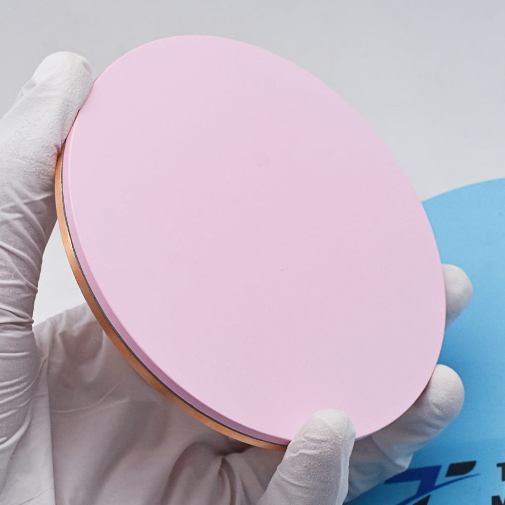
Erbium oxide is a rare earth sesquioxide with the chemical formula Er2O3. It is a pinkish, crystalline solid with a high melting point (approximately 2,340°C), moderate density (~8.64 g/cm3), and excellent chemical stability. These properties make it well-suited for thin film applications that demand durability and robustness under harsh conditions.
Key characteristics:
- Optical Transparency: Er2O3 exhibits a wide optical band gap (5.7–6.0 eV), making it transparent across the visible and near-infrared regions.
- Photoluminescence: The presence of trivalent erbium ions (Er3+) enables strong emission at 1.54 µm, a critical wavelength for optical communications.
- Dielectric Properties: Erbium oxide offers a relatively high dielectric constant, which is beneficial in microelectronics.
- Thermal Stability: The material maintains its structure and properties even at elevated temperatures, a necessity for advanced device fabrication.
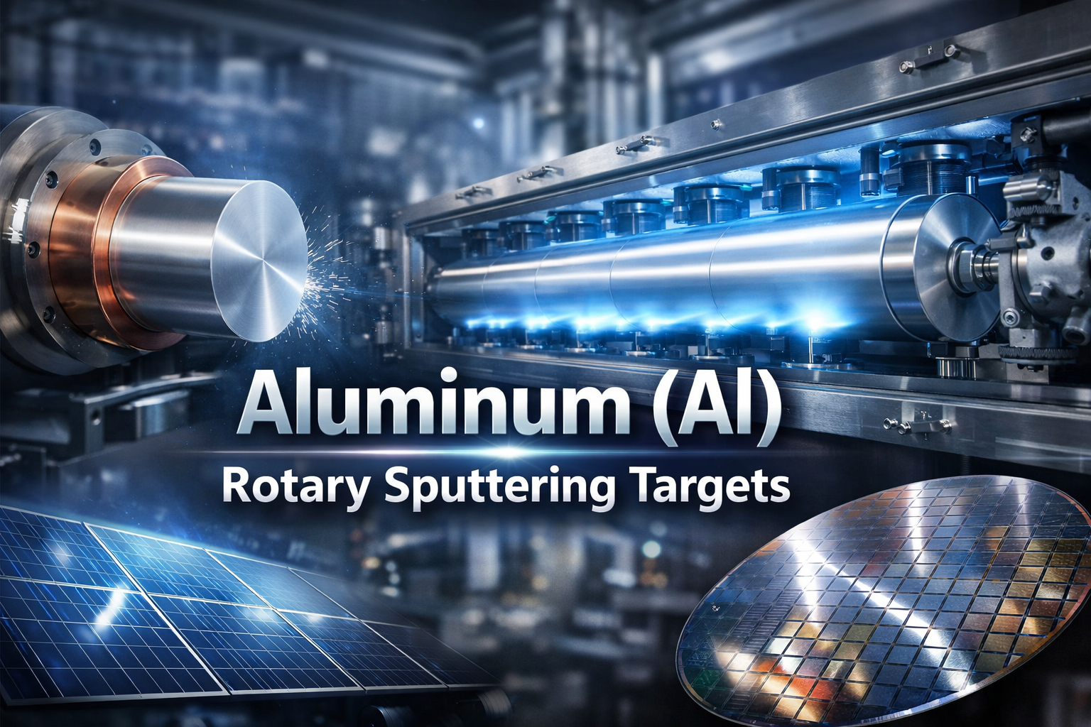
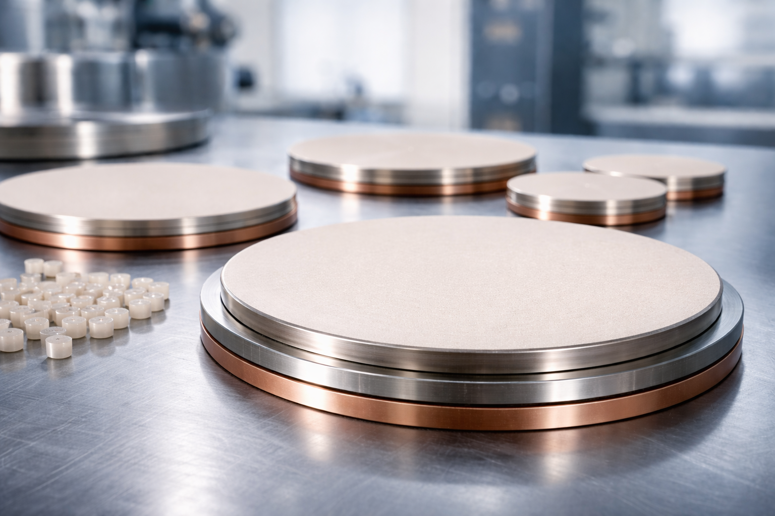
Erbium Oxide Sputtering Target Manufacturing
Producing a high-quality erbium oxide sputtering target involves several steps:
- Powder Preparation: High-purity erbium oxide powder is synthesized or procured, with impurity levels as low as parts-per-million (ppm) to ensure device-grade films.
- Compaction and Sintering: The powder is compacted into a desired shape (typically discs or rectangles) under high pressure and then sintered at temperatures above 1,500°C to achieve high density and mechanical strength.
- Machining: The sintered target is machined to precise dimensions and surface finishes compatible with sputtering systems.
- Bonding (if necessary): For large or thin targets, bonding to a backing plate (often copper or molybdenum) is performed to enhance thermal conductivity and mechanical integrity during sputtering.
Thin Film Deposition by Sputtering
Sputtering Fundamentals
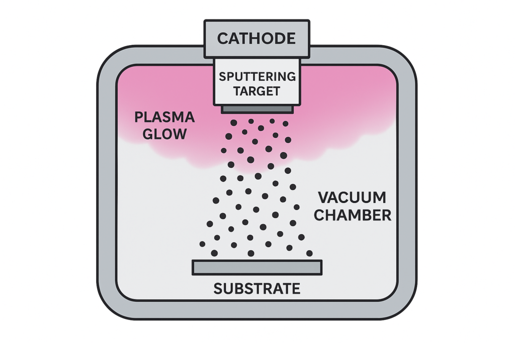
Sputtering is a physical vapor deposition (PVD) technique where energetic ions (typically Ar+) generated in a plasma bombard the target material, causing atoms or molecules to be ejected and subsequently deposited onto a substrate. Sputtering is widely used for producing high-purity, uniform, and adherent thin films.
There are several sputtering configurations, with RF magnetron sputtering and DC sputtering being particularly relevant for oxides like Er2O3. The choice depends on the electrical conductivity of the target and the desired film properties.
Sputtering Process Parameters
Key parameters influencing the deposition of erbium oxide thin films include:
- Target purity and density
- Base pressure and working gas (Ar, O2)
- Power input (RF or DC, typically 50–300 W)
- Substrate temperature (ambient to 600°C or higher)
- Deposition rate and film thickness control
- Oxygen partial pressure (critical for stoichiometry)
Optimizing these parameters ensures high-quality, stoichiometric, and uniform erbium oxide films suitable for demanding photonic and semiconductor applications.
Advantages of Sputtering Erbium Oxide
- Excellent Film Uniformity: Magnetron sputtering enables large-area uniform coatings, essential for industrial-scale fabrication.
- Precise Thickness Control: Sputtering allows sub-nanometer control over film thickness, critical for optical and electronic device performance.
- Strong Film Adhesion: The energetic nature of sputtered species leads to dense, adherent films even on challenging substrates (glass, silicon, polymers).
- Versatility: Compatible with a wide range of substrates and can be tuned for various microstructural and optical properties by adjusting process parameters.
Applications in Photonics
Optical Amplifiers and Waveguides
Erbium oxide’s most celebrated application in photonics lies in its use as a dopant or active layer in optical amplifiers and waveguides. The 1.54 µm emission of Er3+ ions coincides with the minimum loss window of silica optical fibers, making Er2O3-based thin films indispensable in telecommunications.
- Erbium-Doped Waveguide Amplifiers (EDWAs): Thin films of Er2O3 are deposited onto substrates such as silicon oxide or phosphate glass to fabricate compact, integrated optical amplifiers for photonic circuits.
- Planar Lightwave Circuits (PLCs): Incorporating erbium oxide layers enables on-chip amplification, essential for high-bandwidth data transmission.
- Photonic Integrated Circuits: Erbium oxide thin films are integrated with silicon photonics for next-generation optical interconnects, lasers, and modulators.
Optical Information Storage
The unique optical characteristics of erbium oxide make it valuable in the optical information storage industry. Thin films act as active or sensitizing layers in rewritable optical disks (CDs, DVDs), holographic storage, and high-density data recording devices. The films’ stability and high refractive index are leveraged to improve storage density and data retrieval speed.
Display Technology and LEDs
Erbium oxide thin films serve as functional layers in advanced display technologies and light-emitting diodes (LEDs).
- Color Filters and Pixel Layers: The pinkish hue and emission properties of Er2O3 are exploited in color filter arrays for displays, contributing to vivid color rendering and improved efficiency.
- Phosphors for LEDs: Erbium oxide is used as a host or activator in phosphor materials, enhancing the emission characteristics of LEDs for lighting and display applications.
- Transparent Conductive Films: When combined with other oxides, erbium oxide enables the creation of transparent, conductive, and optically active layers in next-generation display panels.
Glass Coatings for Automotive and Architectural Applications
The durability and optical transparency of erbium oxide thin films are harnessed in glass coatings for automotive and architectural purposes. These coatings offer:
- UV and IR Filtering: Improved energy efficiency and passenger comfort in vehicles and buildings.
- Decorative Effects: Subtle coloration and reflective properties for aesthetic enhancement.
- Scratch and Weather Resistance: Protection of glass surfaces in harsh environments.
Optical Communication Systems
Erbium oxide thin films are pivotal in the evolution of optical communication systems. Their integration into planar waveguides, fiber lasers, and amplifiers enables:
- Signal Amplification: Low-noise, high-gain amplification at the C-band (1530-1565 nm) in fiber-optic networks.
- Wavelength Conversion: Nonlinear optical processes in erbium-based films facilitate wavelength division multiplexing (WDM) and signal routing.
- Integrated Photonic Devices: Miniaturization and integration of optical functions on a single chip for data centers and telecommunication infrastructure.
Applications in Semiconductors
High-k Dielectric Layers
As device dimensions continue to shrink, the demand for high-permittivity (high-k) dielectrics rises. Erbium oxide is a promising candidate for replacing silicon dioxide and other conventional dielectrics in semiconductor transistors, capacitors, and memory cells.
- Gate Dielectrics: Er2O3 thin films offer a high dielectric constant, low leakage currents, and excellent thermal stability, making them suitable for gate stacks in advanced metal-oxide-semiconductor field-effect transistors (MOSFETs).
- DRAM and Flash Memory: The use of erbium oxide as an insulating layer improves the charge retention, scaling, and reliability of dynamic and non-volatile memories.
Semiconductor Passivation and Encapsulation
The chemical inertness and impermeability of erbium oxide films make them ideal for passivating and encapsulating sensitive semiconductor devices. These films protect active regions from atmospheric moisture, oxygen, and contaminants, thereby enhancing device longevity and stability.
Functional Coatings and Sensor Devices
Erbium oxide thin films are employed as functional coatings in microelectromechanical systems (MEMS), biosensors, and gas sensors. Their stability, optical response, and compatibility with silicon technology enable new sensor architectures with improved sensitivity and selectivity.
Decorative and Antireflective Coatings
In addition to functional roles, erbium oxide’s optical properties are utilized in decorative and antireflective coatings for semiconductor devices, smart windows, and photovoltaic modules. These coatings enhance device efficiency while providing attractive visual effects.
Thin Film Deposition Techniques and Process Optimization
Sputtering System Types
There are several sputtering methods suitable for depositing erbium oxide films:
- RF Magnetron Sputtering: Preferred for insulating targets like Er2O3, enabling high deposition rates and uniform films on large substrates.
- Pulsed DC Sputtering: Useful for reactive processes and reducing target arcing.
- Reactive Sputtering: Metallic erbium targets are sputtered in an oxygen-containing atmosphere to form Er2O3 films in-situ, allowing precise stoichiometry control.
Process Parameters and Their Effects
- Substrate Temperature: Higher temperatures promote better film crystallinity, adhesion, and lower defect densities, but may not be compatible with all substrates.
- Oxygen Partial Pressure: Controls the stoichiometry and phase purity of the deposited film. Excess oxygen can lead to over-oxidation or porous films, while insufficient oxygen may result in sub-stoichiometric phases or metallic inclusions.
- Power and Deposition Rate: Adjusting the RF or DC power affects the energy and flux of sputtered species, influencing film density and microstructure.
- Post-Deposition Annealing: Thermal treatment can improve film crystallinity, reduce defects, and enhance optical and electrical properties.
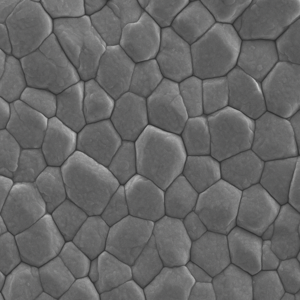
Film Characterization and Quality Control
Ensuring the performance of erbium oxide thin films requires comprehensive characterization:
- X-ray Diffraction (XRD): Identifies crystal structure and phase purity.
- Scanning Electron Microscopy (SEM) and Atomic Force Microscopy (AFM): Assess surface morphology and roughness.
- Spectroscopic Ellipsometry: Measures film thickness and optical constants (refractive index, extinction coefficient).
- X-ray Photoelectron Spectroscopy (XPS): Determines chemical composition and oxidation states.
- Photoluminescence Spectroscopy: Evaluates emission properties, essential for photonic applications.
Comparative Analysis: Erbium Oxide vs. Other Rare Earth Oxides
Material Selection in Thin Film Technology
While erbium oxide is highly valued for its photonic and semiconductor applications, other rare earth oxides such as europium oxide (Eu2O3), cerium oxide (CeO2), holmium oxide (Ho2O3), and dysprosium oxide (Dy2O3) are also utilized in thin film technology. Each offers distinct optical, electronic, and chemical properties suited to specific applications.
- Europium Oxide: Excellent red phosphor emitter, widely used in displays and lighting.
- Cerium Oxide: High oxygen storage capacity, used in catalysis and transparent conductive coatings.
- Holmium and Dysprosium Oxides: Strong magnetic and Faraday rotation effects, used in magneto-optic devices.
- Erbium Oxide: Unique for its 1.54 µm emission, making it irreplaceable in optical communication applications.
The choice of oxide depends on the targeted optical transitions, dielectric properties, and compatibility with device architectures.
Industrial and Research Applications
Semiconductor Fabrication
In the semiconductor industry, erbium oxide sputtering targets are integral to the fabrication of advanced logic and memory chips, sensors, and optoelectronic devices. Their use enables:
- Scaling of CMOS Devices: Replacement of conventional dielectrics with erbium oxide for continued miniaturization and performance improvement.
- On-chip Photonics: Integration of erbium oxide films for light emission, amplification, and detection directly on silicon chips.
Display and LED Manufacturing
Erbium oxide thin films contribute to the advancement of high-resolution, energy-efficient displays and LEDs by serving as color filters, emission layers, and antireflective coatings. Their stability and emission characteristics are leveraged to realize vibrant, long-lasting display panels for consumer electronics, automotive dashboards, and industrial instrumentation.
Photovoltaic Devices
The photovoltaic industry benefits from erbium oxide’s optical and dielectric properties in several ways:
- Antireflective Coatings: Maximizing light absorption and conversion efficiency in solar cells.
- Upconversion Layers: Erbium oxide films can upconvert sub-bandgap infrared photons to higher-energy photons, enhancing the spectral response of silicon solar cells.
Optical Information Storage
Erbium oxide’s stability and optical response make it a preferred choice for rewritable optical disks, holographic storage materials, and next-generation archival media. The films’ robustness ensures data integrity and longevity.
Glass Coating Industry
In automotive and architectural glass, erbium oxide thin films are applied to improve energy efficiency, durability, and aesthetics. The films provide UV/IR filtering, color tuning, and weather resistance, significantly enhancing the performance and appearance of glazing products.
Packaging and Handling of Erbium Oxide Sputtering Targets
Packaging Requirements
Erbium oxide sputtering targets are typically packaged to preserve their purity, prevent contamination, and ensure mechanical integrity during transit and storage. Common packaging practices include:
- Vacuum-sealed or inert gas-filled packaging to prevent moisture uptake and oxidation.
- Shock-absorbing materials and rigid containers to protect against mechanical damage.
- Labeling with batch numbers, purity grades, and dimensions for traceability and process control.
Storage and Handling
- Store in a clean, dry environment, away from corrosive chemicals and humidity.
- Use gloves and clean tools when handling to avoid contamination.
- Bonded targets (those attached to backing plates) should be handled with additional care to avoid delamination.
Future Trends and Research Directions
Nanostructured and Co-doped Erbium Oxide Films
Research is ongoing to develop nanostructured erbium oxide films and co-doped systems (e.g., Er-Yb, Er-Tm) to enhance emission efficiency, bandwidth, and energy transfer for photonic applications. These materials promise higher performance in quantum photonics, lasers, and amplifiers.
Integration with Silicon Photonics
The push towards monolithic integration of photonic and electronic components on silicon platforms drives the need for erbium oxide films with controlled microstructure, low defect density, and tailored optical properties. Advances in deposition and processing techniques are key to realizing high-yield, scalable production.
Advanced Characterization and Modeling
State-of-the-art analytical tools and computational modeling are being employed to understand the fundamental mechanisms governing erbium oxide thin film growth, defect formation, and energy transfer processes. This knowledge will inform the design of next-generation materials and devices.
Green Manufacturing and Recycling
Sustainability is increasingly important in thin film manufacturing. Efforts are underway to develop greener synthesis routes for erbium oxide, improve target recycling, and minimize waste in sputtering processes.
Conclusion
The erbium oxide sputtering target stands at the forefront of thin film material science, underpinning advances in photonics and semiconductors. Its unique combination of optical, dielectric, and chemical properties enables the fabrication of high-performance devices for telecommunications, data storage, displays, energy, and beyond.
Through continued innovation in material synthesis, deposition technology, and application engineering, erbium oxide will maintain its pivotal role in the evolution of modern electronics and photonics. As demands for faster, more efficient, and miniaturized devices grow, the importance of high-purity, well-engineered erbium oxide sputtering targets will only increase, driving progress across multiple high-tech industries.