Introduction
The global energy landscape is undergoing one of the most transformative decades in history. Driven by the urgent need for carbon neutrality, the solar industry continues to diversify beyond conventional crystalline silicon (c-Si) modules. A new generation of thin-film photovoltaic (TFPV) technologies—such as perovskite, CIGS (Cu(In,Ga)Se₂), and CdTe (Cadmium Telluride)—is gaining significant traction for their lightweight, flexible, and high-efficiency potential.
From wearable electronics and building-integrated photovoltaics (BIPV) to space and mobile applications, thin-film solar materials are redefining what solar power can look like and where it can be deployed. This article explores the latest trends, material challenges, and the vital role of advanced sputtering and evaporation materials—TFM’s expertise—in supporting this fast-evolving industry.
1. Market Overview: A New Growth Wave
According to recent analyses from IDTechEx and Allied Market Research, the global thin-film photovoltaic market is projected to grow from USD 12 billion in 2024 to over USD 22 billion by 2030, with a CAGR exceeding 10 %.
Key Growth Drivers
- Lightweight and Flexible Design:
Thin-film devices are typically 90 % thinner than crystalline silicon wafers, making them ideal for integration on curved or lightweight substrates. - Manufacturing Cost Advantage:
Lower material consumption and the potential for roll-to-roll (R2R) processing enable higher throughput and reduced cost per watt. - Emerging Applications:
Demand surges in wearable devices, IoT sensors, automotive rooftops, and BIPV façade modules. - Energy Transition Policies:
The EU Green Deal, China’s 14th Five-Year Plan, and the U.S. IRA (Inflation Reduction Act) all include incentives for advanced solar manufacturing, including TFPV lines.
Major Players and Geographic Trends
- CdTe: First Solar (USA) remains the dominant player, expanding its U.S. capacity.
- CIGS: Europe and Japan (Solar Frontier, Avancis) continue refining efficiency and scaling R2R coating lines.
- Perovskite: China, South Korea, and UK start-ups are driving pilot production with hybrid tandems.
2. Technology Families: CdTe, CIGS, and Perovskite
2.1 CdTe Thin-Film Solar Cells
CdTe is one of the most mature thin-film technologies, recognized for:
- High absorption coefficient and optimal bandgap (≈ 1.45 eV).
- Simplified layer stack: typically glass / TCO / CdS / CdTe / back contact.
- Production scalability with high throughput vacuum deposition.
Material Challenges:
- Cadmium toxicity demands strict recycling and encapsulation.
- Maintaining high-purity Cd and Te sputtering targets (4N–5N) is critical for film uniformity and carrier mobility.
- Alternative back contacts (Cu-free) are under investigation to prevent diffusion and long-term degradation.
2.2 CIGS (Cu (In, Ga) Se₂) Solar Cells
CIGS offers high absorption and excellent radiation tolerance, making it attractive for space and mobile power.
The core layer is usually deposited by co-evaporation or magnetron sputtering using Cu–In–Ga–Se alloy targets.
Advantages
- Tunable bandgap (1.0–1.7 eV) via Ga content.
- Compatibility with flexible polymer or metal-foil substrates.
- Superior aesthetics and bending tolerance compared to crystalline modules.
Material Challenges
- Complex stoichiometry control: deviations of ± 1 at % can reduce efficiency by > 5 %.
- Selenium volatility and uniformity issues in large-area sputtering.
- High-purity targets (99.999 %) required for consistent layer thickness and composition.
- Buffer layer (CdS or Zn(O,S)) optimization critical for junction quality.
2.3 Perovskite Solar Cells (PSCs)
Perovskite materials (ABX₃ structure, typically CH₃NH₃PbI₃) have demonstrated record efficiencies over 26 % in lab settings and are compatible with low-temperature deposition.
Key Features
- Solution or vacuum deposition processes enable lightweight, flexible devices.
- Potential to integrate with Si or CIGS tandems for > 30 % efficiency.
- Compatible with transparent electrodes for semi-transparent or curved modules.
Challenges
- Moisture and UV instability remain major hurdles.
- Scaling from 1 cm² to 1 m² introduces uniformity and defect-density problems.
- Lead toxicity concerns drive research into lead-free perovskites (Sn-based).
- Requires high-purity oxide and halide sputtering targets (e.g., SnO₂, ITO, NiOx, MoOx) to achieve stable interface layers.
3. Applications: From BIPV to Wearable Energy
3.1 Building-Integrated Photovoltaics (BIPV)
BIPV is one of the fastest-growing markets for TFPV.
Thin, light, and aesthetic films (e.g., CIGS, perovskite) can be laminated into façades, rooftops, or glass panels.
For architects and developers, TFPV provides a functional + decorative energy solution.
Material Enablers
- Transparent conductive oxides (TCOs) such as ITO, AZO, FTO.
- High-purity metal back contacts (Mo, Ni, Ag).
- Durable encapsulation materials compatible with architectural glazing.
3.2 Flexible and Wearable Solar Electronics
Applications extend to:
- Smartwatches, textile-integrated sensors, IoT nodes.
- Foldable drones and mobile power devices.
Requirements
- Bending radius < 5 mm.
- Low-temperature deposition (< 150 °C) to protect polymer substrates.
- Conductive but transparent electrodes—Ag nanowire or graphene-based coatings gaining popularity.
3.3 Automotive and Aerospace Integration
CIGS and perovskite modules are increasingly used for curved vehicle roofs or aerospace payloads.
- Weight reduction of 40–60 % compared to crystalline silicon.
- Radiation-resistant and high power-to-weight ratio (150–250 W/kg).
- Ideal for drones, satellites, and electric aircraft.
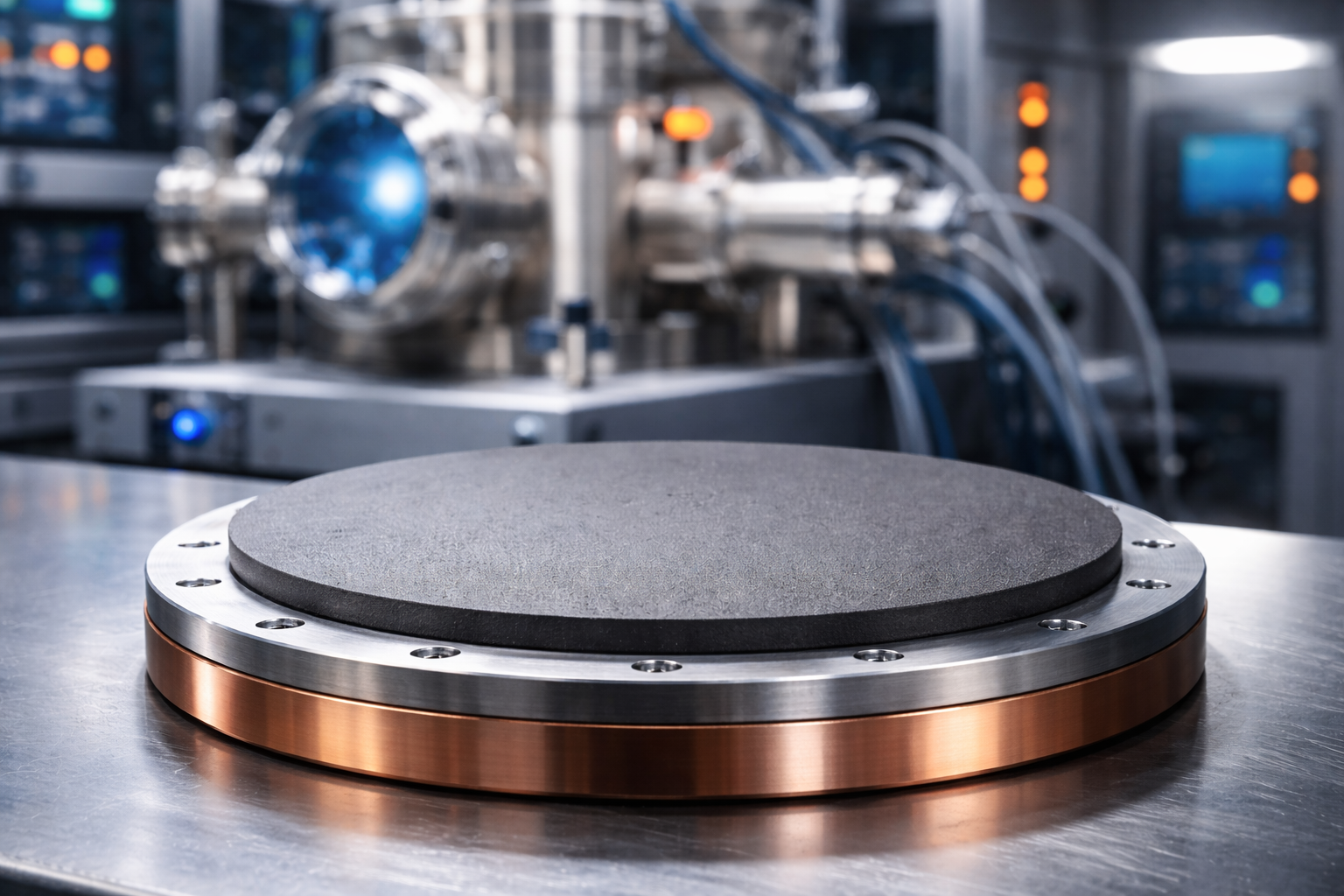
4. Role of Advanced Sputtering and Evaporation Materials
Thin-film solar devices rely heavily on high-purity sputtering targets and evaporation materials.
At TFM, such materials form the foundation of each functional layer—from TCO electrodes to absorber and buffer interfaces.
| Film Layer | Common Material | Deposition Method | Notes |
|---|---|---|---|
| Transparent Electrode | ITO, AZO, FTO | Sputtering | Optical transmittance > 85 % |
| Absorber Layer | CdTe, CIGS, Perovskite | Co-evaporation / Sputtering | Precise stoichiometry control needed |
| Buffer Layer | CdS, Zn(O,S), TiO₂ | RF Sputtering | Thin (50–100 nm) for optimal junction |
| Back Contact | Mo, Ni, Ag, Carbon | DC Sputtering / Thermal Evaporation | Conductivity and adhesion critical |
| Encapsulation | Al₂O₃, SiO₂ | ALD / PVD | Barrier against moisture and UV |
Why Material Purity Matters:
Impurities > 50 ppm can alter carrier lifetime or introduce non-radiative recombination centers, reducing efficiency and device stability.
TFM’s targets (3N to 6N purity) ensure consistent film density, composition uniformity, and repeatable optical/electrical properties.
5. Material and Process Challenges
Despite rapid progress, several technical barriers remain before mass adoption.
5.1 Scalability
Moving from lab-scale to roll-to-roll industrial production requires high-deposition uniformity over > 1 m² substrates.
Precision-engineered sputtering targets and optimized deposition parameters are key to achieving consistent layer properties.
5.2 Material Stability
Perovskite films are vulnerable to moisture, oxygen, and UV light.
Advanced encapsulation and barrier layers (e.g., Al₂O₃ and SiNₓ) are crucial to reach > 20-year lifetimes.
5.3 Environmental and Safety Concerns
Cd and Pb toxicity requires closed-loop manufacturing and recycling protocols.
TFM supports environmentally responsible production with traceable source materials and cleanroom processing.
5.4 Efficiency Degradation
Ion migration and interface defects cause gradual efficiency loss.
Research into stable inorganic buffer layers and diffusion barriers continues to reduce degradation rates.
6. Market Outlook 2025–2030
| Region | Expected CAGR (2025–2030) | Key Driver |
|---|---|---|
| Asia-Pacific | > 12 % | Perovskite pilot lines and EV integration |
| Europe | 10 % | BIPV and green building initiatives |
| North America | 9 % | IRA incentives and domestic CdTe capacity |
| Middle East / Africa | 8 % | Off-grid and mobile power applications |
The trend is clear: flexible and thin-film photovoltaics will complement, not replace, traditional silicon. Their value lies in design freedom, integration, and specific performance advantages where rigid panels cannot compete.
7. TFM’s Perspective and Solutions
As a specialist in high-purity sputtering and evaporation materials, TFM serves thin-film solar manufacturers worldwide with materials designed for next-generation efficiency and stability.
7.1 Advanced Target Materials
- CIGS and CZTS Targets: Custom stoichiometry and densification for uniform film growth.
- Perovskite Interface Materials: ITO, NiOx, SnO₂, TiO₂ targets with > 99.99 % purity.
- TCO Solutions: Tailored AZO and FTO targets for high transparency and low resistivity.
7.2 Process Support
TFM provides process consulting for deposition parameters, bonding methods, and target life optimization—helping customers achieve maximum yield and film uniformity.
7.3 Sustainability Initiatives
Through recycling and refining programs, TFM reclaims spent targets to reduce waste and support the industry’s circular economy goals.
8. Future Directions
- Perovskite + Silicon Tandems will reach > 30 % efficiency with vacuum-deposited layers.
- Flexible CIGS Modules on polyimide substrates will expand into automotive and aerospace markets.
- Lead-free perovskite research (Sn, Ge systems) will be commercially viable by 2028.
- Roll-to-roll manufacturing will lower cost to < USD 0.20 per watt by 2030.
- Advanced thin-film barriers and AI-controlled coating lines will extend device lifetimes beyond 25 years.
Conclusion
Flexible and thin-film photovoltaic technologies represent a dynamic intersection of material science, renewable energy policy, and design innovation.
As CIGS, CdTe, and perovskite technologies converge toward commercial maturity, their success will hinge on one foundation—advanced deposition materials that deliver purity, stability, and precision.
TFM (Thin Film Materials) is committed to supporting this revolution through continuous innovation in sputtering targets and evaporation materials, enabling the next generation of clean, lightweight, and flexible solar power solutions.
You May Also Want to Know
- What is the efficiency limit of thin-film solar cells?
Theoretical Shockley-Queisser limit ≈ 33 %, but tandems can surpass 40 %. - Are thin-film cells recyclable?
Yes—especially CdTe and CIGS; recycling reclaims Cd, Te, In, Ga metals. - How do perovskite cells achieve such high efficiencies?
Through tunable bandgap and defect tolerance within the crystal lattice. - Why are flexible substrates important?
They enable curved, lightweight designs for wearables and BIPV. - What role do sputtering targets play in solar fabrication?
They define film composition, uniformity, and electrical performance. - Are perovskite solar cells commercially available yet?
Pilot production began in 2024; mass deployment expected around 2026–2027. - Can thin-film cells work under low-light conditions?
Yes; they often perform better than silicon under diffuse light. - Which thin-film technology is most cost-effective today?
CdTe still leads in levelized cost of energy (LCOE), around USD 0.03/kWh. - What is the main environmental concern?
Heavy metal toxicity; proper encapsulation and recycling solve most risks. - How does TFM support solar manufacturers globally?
Through high-purity target supply, custom R&D collaboration, and responsive technical service.