
Introduction
Alumina Ceramic Substrates (Al₂O₃) are among the most widely used technical ceramic materials in electronics, thin film deposition, and high-temperature applications. Known for their excellent electrical insulation, high thermal conductivity, mechanical strength, and chemical stability, alumina substrates provide a reliable platform for the fabrication of electronic circuits, sensors, and thin film devices.
Due to their outstanding performance under harsh environmental conditions, Al₂O₃ ceramic substrates are commonly used in semiconductor manufacturing, hybrid circuits, power electronics, and vacuum deposition processes. Their dimensional stability and compatibility with a wide range of thin film coating techniques make them an essential component in modern electronic and materials engineering applications.
Detailed Description
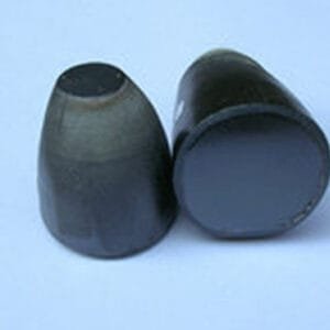
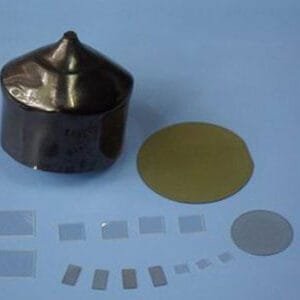
Alumina ceramic substrates are manufactured from high-purity aluminum oxide (Al₂O₃) powders through advanced ceramic processing techniques such as tape casting, pressing, and high-temperature sintering. The resulting substrates exhibit dense microstructures, excellent mechanical strength, and superior thermal and electrical performance.
One of the key advantages of alumina substrates is their combination of electrical insulation and thermal conductivity. While the material acts as an excellent dielectric insulator, it simultaneously provides efficient heat dissipation. This makes Al₂O₃ substrates ideal for electronic devices where thermal management is critical, such as power modules and integrated circuits.
Alumina substrates are also highly resistant to chemical corrosion and oxidation, allowing them to maintain stable performance even in aggressive environments or high-temperature conditions. Depending on the purity level, alumina substrates can withstand temperatures exceeding 1000 °C without significant structural degradation.
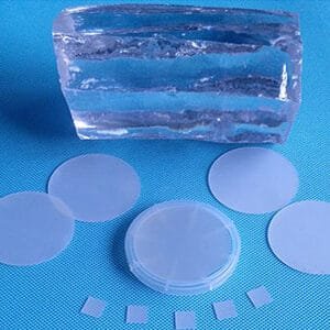
Surface quality is another important feature of Al₂O₃ substrates. They are typically manufactured with smooth, flat surfaces that are suitable for thin film deposition methods such as sputtering, evaporation, chemical vapor deposition (CVD), and screen printing. High surface flatness and low roughness help ensure uniform coating thickness and strong film adhesion.
Different purity grades—such as 96%, 99%, and 99.6% alumina—are available to meet different application requirements. Higher purity alumina generally provides improved thermal conductivity, better dielectric performance, and enhanced mechanical stability.
Alumina ceramic substrates can also be customized in terms of dimensions, thickness, surface finishing, and metallization patterns, making them suitable for a wide range of industrial and research applications.
Applications
Alumina Ceramic Substrates are used in numerous industries due to their reliable electrical and thermal properties. Typical applications include:
Thin film deposition substrates for sputtering, evaporation, and CVD coatings
Hybrid microelectronics and integrated circuits
Power electronics modules and heat-dissipating circuit boards
Sensors and MEMS devices
LED and optoelectronic device packaging
RF and microwave electronic components
High-temperature electronic systems
These substrates serve as stable platforms for the fabrication of advanced electronic and thin film devices.
Technical Parameters
| Parameter | Typical Value / Range | Importance |
|---|---|---|
| Purity | 96% – 99.6% Al₂O₃ | Higher purity improves thermal and electrical performance |
| Density | ≥ 3.7 g/cm³ | High density ensures mechanical strength |
| Surface Roughness | Ra ≤ 0.5 μm (polished available) | Important for thin film uniformity |
| Thickness | 0.25 – 2 mm (custom available) | Determines mechanical and thermal properties |
| Thermal Conductivity | 20 – 30 W/m·K | Helps dissipate heat in electronic devices |
| Dielectric Strength | >15 kV/mm | Provides excellent electrical insulation |
Comparison with Related Materials
| Material | Key Advantage | Typical Application |
|---|---|---|
| Alumina (Al₂O₃) | Excellent insulation and thermal stability | Electronics substrates and thin film deposition |
| Aluminum Nitride (AlN) | Higher thermal conductivity | High-power electronics |
| Silicon (Si) | Semiconductor functionality | Integrated circuits |
| Sapphire (Al₂O₃ single crystal) | Superior optical transparency | Optical devices and LEDs |
FAQ
| Question | Answer |
|---|---|
| Can alumina ceramic substrates be customized? | Yes, size, thickness, surface finish, and purity levels can be customized according to application requirements. |
| What thin film deposition methods are compatible with Al₂O₃ substrates? | Alumina substrates are compatible with sputtering, evaporation, chemical vapor deposition (CVD), and other coating techniques. |
| What purity levels are commonly available? | Typical purity grades include 96%, 99%, and 99.6% alumina. |
| Are alumina substrates suitable for high temperatures? | Yes, they can withstand temperatures above 1000 °C depending on the purity and application conditions. |
| What industries use alumina substrates most? | Semiconductor, electronics manufacturing, sensors, power devices, and materials research. |
Packaging
Our Alumina Ceramic Substrate (Al₂O₃) are meticulously tagged and labeled externally to ensure efficient identification and maintain high standards of quality control. We take great care to prevent any potential damage during storage and transportation, ensuring the targets arrive in perfect condition.
Conclusion
Alumina Ceramic Substrates (Al₂O₃) provide an excellent balance of electrical insulation, thermal conductivity, mechanical strength, and chemical stability. These properties make them one of the most reliable substrate materials for electronics, thin film deposition, and high-temperature applications.
With customizable sizes, purity levels, and surface finishes, alumina substrates can be tailored to meet the requirements of modern semiconductor manufacturing and advanced materials research.
For detailed specifications and a quotation, please contact us at sales@thinfilmmaterials.com.
Reviews
There are no reviews yet.