
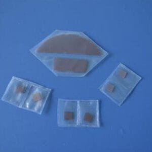
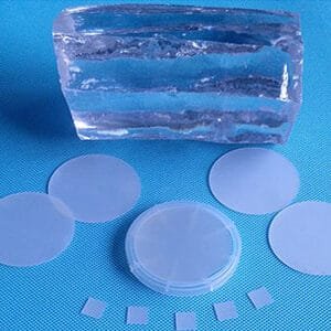
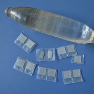
Aluminum Nitride Ceramic Substrate
The Aluminum Nitride (AlN) ceramic substrate is known for its exceptional thermal conductivity, superior electrical properties, high mechanical strength, and excellent resistance to high temperatures. Its chemical corrosion resistance, high electrical resistivity, low dielectric loss, and non-toxic nature make it an outstanding alternative to BeO ceramics. Due to these advantages, AlN substrates are widely used in high-density hybrid circuits, microwave power devices, power electronics, optoelectronic components, and semiconductor refrigeration systems.
Physical Properties of Aluminum Nitride Ceramic Substrate
| Property | Value |
|---|---|
| Material | AlN |
| Density (g/cm³) | 3.335 |
| Hardness (Mohs) | 8 |
| Thermal Conductivity (W/m.K) | 180 |
| Thermal Expansion (x10⁻⁶/°C) | 4.0 |
| Dielectric Constant (at 1 MHz) | 8.8 |
| Flexural Strength (N/mm²) | 450 |
Specifications
- Standard Size: 100 x 100 x 1.0 mm
- Customization: Available upon request
- Polish Options: SSP or DSP
- Surface Roughness (Ra): 0.01 to 0.7 µm
Applications
Aluminum Nitride ceramic substrates are used in various industries, including:
- Automotive Electronics: Ideal for advanced electronic components
- Semiconductor Refrigeration Devices: Efficient heat dissipation solutions
- LED Lighting: Enhancing thermal management for high-performance lighting systems
- Power Resistors: Suitable for high-power applications
With superior thermal and mechanical properties, Aluminum Nitride ceramic substrates are a reliable choice for demanding industrial applications.
Reviews
There are no reviews yet.