Introduction
Antimony Doped Tin Oxide Evaporation Materials (ATO Evaporation Materials) are functional oxide compounds designed for the deposition of transparent conductive and infrared-reflective thin films. By introducing antimony (Sb) into tin oxide (SnO₂), electrical conductivity is significantly enhanced while maintaining high optical transparency.
ATO thin films are widely applied in optoelectronics, energy-saving glass, display technologies, and electrostatic protection coatings. In vacuum evaporation systems, high-purity ATO materials ensure stable composition transfer and reliable film performance.
Detailed Description
ATO is a doped semiconductor oxide in which antimony acts as an n-type dopant within the SnO₂ lattice. The Sb concentration (commonly 5–15 wt% Sb₂O₃ equivalent) directly influences electrical conductivity and optical properties.
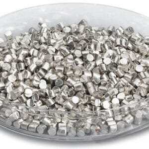
Evaporation materials are typically supplied as:
Sintered pellets
Granules
Pressed tablets
Custom-shaped pieces for crucibles
Manufacturing emphasizes:
Controlled Sb doping level for consistent conductivity
High phase purity to prevent secondary phase formation
Dense microstructure to improve evaporation stability
Optimized particle size for uniform heating
ATO evaporation materials are compatible with thermal evaporation and electron beam evaporation systems. Oxygen partial pressure control during deposition may be required to maintain appropriate film stoichiometry and optimize carrier concentration.
The resulting ATO films typically exhibit:
High optical transparency in the visible range
Improved electrical conductivity compared to pure SnO₂
Infrared reflection properties
Good chemical and thermal stability
These characteristics make ATO a practical alternative to other transparent conductive oxides in specific cost-sensitive applications.
Applications
Antimony Doped Tin Oxide Evaporation Materials are widely used in:
Transparent conductive coatings
Low-emissivity (Low-E) glass coatings
Touch panels and display technologies
Antistatic coatings
Solar cell front electrodes (research and niche applications)
Electrochromic devices
Optical and functional oxide thin films
ATO films are often used in architectural glass and automotive glazing to improve energy efficiency through infrared reflection.
Technical Parameters
| Parameter | Typical Value / Range | Importance |
|---|---|---|
| Chemical Composition | SnO₂:Sb₂O₃ (custom ratio) | Determines electrical conductivity |
| Sb Doping Level | 5–15 wt% typical | Controls carrier concentration |
| Purity | 99.9% – 99.99% | Reduces optical absorption losses |
| Form | Pellets / Granules / Pieces | Compatible with evaporation sources |
| Density | ≥ 95% theoretical | Improves deposition stability |
| Deposition Method | Thermal / E-beam Evaporation | Ensures uniform thin film growth |
Custom compositions and pellet sizes can be supplied to match specific system configurations.
Comparison with Related Transparent Conductive Oxides
| Material | Key Advantage | Typical Application |
|---|---|---|
| ATO | Cost-effective conductivity & IR reflection | Low-E glass & antistatic films |
| ITO (Indium Tin Oxide) | High conductivity & transparency | Displays & touch panels |
| FTO (Fluorine Doped Tin Oxide) | Thermal stability | Solar glass |
| AZO (Aluminum Doped Zinc Oxide) | Indium-free alternative | Transparent electrodes |
Compared to ITO, ATO offers a lower-cost alternative with good infrared reflection performance, especially in architectural glass applications.
FAQ
| Question | Answer |
|---|---|
| Can the Sb doping ratio be customized? | Yes, doping levels can be tailored to achieve desired conductivity and transparency. |
| Is oxygen control required during deposition? | Yes, controlling oxygen partial pressure can optimize film properties. |
| Is ATO suitable for transparent conductive coatings? | Yes, it is widely used for conductive and antistatic thin films. |
| Can it replace ITO? | In certain cost-sensitive or IR-reflective applications, ATO can be a viable alternative. |
| Do you provide material certification? | Yes, chemical composition and batch traceability documents are available. |
Packaging
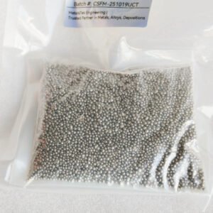
Our Antimony Doped Tin Oxide Evaporation Materials are meticulously tagged and labeled externally to ensure efficient identification and maintain high standards of quality control. We take great care to prevent any potential damage during storage and transportation, ensuring the materials arrive in perfect condition.
Conclusion
Antimony Doped Tin Oxide Evaporation Materials (ATO) provide a reliable solution for transparent conductive and infrared-reflective thin films. With controlled doping, stable evaporation behavior, and customizable specifications, they support a broad range of optoelectronic and architectural coating applications.
For detailed specifications and a quotation, please contact us at sales@thinfilmmaterials.com.


 MSDS File


Reviews
There are no reviews yet.