
 MSDS File
Antimony Telluride Evaporation Materials Overview
TFM offers premium antimony telluride evaporation materials, featuring the chemical formula Sb2Te3. This high-purity telluride ceramic is essential for ensuring high-quality deposition films in various processes. We produce Sb2Te3 evaporation materials with purity levels reaching up to 99.9995%, utilizing rigorous quality assurance measures to ensure reliability and excellence.
Specifications of Antimony Telluride Evaporation Materials
| Material Type | Antimony Telluride |
| Symbol | Sb2Te3 |
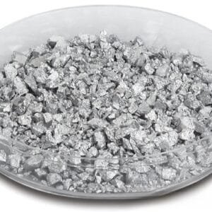
| Appearance/Color | Grey solid |
| Melting Point | 620 °C (1,148 °F; 893 K) |
| Density | 6.50 g cm−3 |
| Purity | 99.9% ~ 99.999% |
| Shape | Powder/ Granule/ Custom-made |
Applications
Antimony telluride evaporation materials are crucial in various deposition techniques, including semiconductor deposition, chemical vapor deposition (CVD), and physical vapor deposition (PVD). They are primarily used in optics for applications such as wear protection, decorative coatings, and displays.
Packaging
Our antimony telluride evaporation materials are securely packed in plastic vacuum bags to protect them during storage and transport, maintaining their quality and integrity. Each package includes a Certificate of Analysis (COA) for the raw material.
Contact Us
At TFM, we excel in producing high-purity antimony telluride evaporation materials tailored for use in semiconductors, CVD, PVD, and optical applications. Our combined expertise in engineering, manufacturing, and analysis ensures we deliver industry-leading products. Contact us today to inquire about our offerings.


Reviews
There are no reviews yet.