
 MSDS File
| Material Type | Arsenic Triselenide |
| Symbol | As2Se3 |
| Melting Point (°C) | ~360 |
| Theoretical Density (g/cc) | 4.75 |
| Z Ratio | |
| E-Beam | |
| E-Beam Crucible Liner Material | |
| Temp. (°C) for Given Vap. Press. (Torr) | |
| Comments |
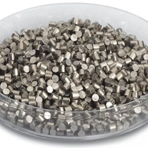
Arsenic Triselenide Pellet Evaporation Material
TFM provides high-purity Arsenic Triselenide (AsSe₃) Pellet Evaporation Material, a crucial compound for thin-film deposition, optoelectronics, and semiconductor research. Known for its exceptional optical and electronic properties, this material is widely used in infrared detectors, photodetectors, and advanced electronic devices.
Key Features and Advantages
High Purity (99.99% – 99.999%) – Ensures superior performance in thin-film deposition and optical applications.
Superior Optical Properties – Provides high transmission and low absorption in the infrared spectrum, ideal for infrared sensors.
Optimized for Thin-Film Deposition – Compatible with thermal evaporation and E-beam evaporation techniques.
Stable & Uniform Coating – Delivers consistent film quality, essential for high-efficiency optoelectronic devices.
Customizable Composition – Tailored to meet specific application needs, allowing for adjustments in optical and electrical performance.
Applications
Infrared Detectors & Sensors – Ideal for thermal imaging and infrared detection in security, military, and scientific applications.
Photodetectors & Photovoltaic Devices – Used in solar cells and optical communication systems.
Thin-Film Transistors & Semiconductor Devices – Applied in transparent electronics, displays, and advanced sensor technologies.
Optoelectronic Devices – Ideal for LEDs, lasers, and optical modulators.
Industry Impact
TFM’s Arsenic Triselenide Pellet Evaporation Material is a high-performance material with outstanding optical and electronic properties, making it indispensable in infrared detection, solar energy, and optoelectronic device fabrication. Its high purity, stable deposition characteristics, and tailored performance make it a top choice for innovative applications in advanced electronics and material research.


Reviews
There are no reviews yet.