 MSDS File
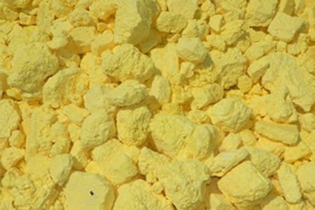
| Material Type | Arsenic Sulfide |
| Symbol | As2S3 |
| Color/Appearance | Orange crystals |
| Melting Point (°C) | 310 |
| Theoretical Density (g/cc) | 3.43 |
| Z Ratio | – |
| E-Beam | Fair |
| Thermal Evaporation Techniques | Boat: Mo Crucible: Al2O3, Q |
| E-Beam Crucible Liner Material | – |
| Temp. (°C) for Given Vap. Press. (Torr) | 10-4: ~400 |
| Comments | – |
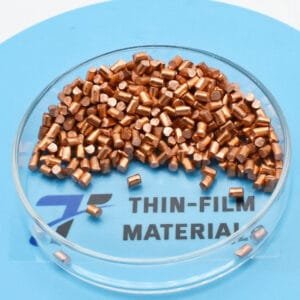
Arsenicum Sulfide Pellet Evaporation Material
TFM offers high-purity Arsenicum Sulfide Pellet Evaporation Material, a versatile compound used in thin-film deposition, optoelectronics, and semiconductor research. Known for its unique optical and electrical properties, this material is widely applied in infrared sensors, photodetectors, and advanced electronic components.
Key Features and Advantages
High Purity (99.99% – 99.999%) – Ensures optimal performance in thin-film deposition and electronic applications.
Superior Optical & Electrical Properties – Ideal for infrared transmission and light-sensitive devices.
Optimized for Thin-Film Deposition – Compatible with thermal evaporation and E-beam evaporation techniques.
Stable & Uniform Coating – Delivers consistent quality in thin-film coatings, crucial for high-efficiency devices.
Customizable Composition – The arsenic/sulfur ratio can be adjusted to meet specific application requirements.
Applications
Infrared Detectors & Sensors – Ideal for thermal imaging and infrared detection in military, medical, and industrial applications.
Photodetectors – Used in light-sensitive devices and optical communication systems.
Semiconductor Research – Supports cutting-edge material science in electronic devices and sensor technologies.
Thin-Film Solar Cells – Applied in photovoltaic devices to enhance solar energy conversion efficiency.
Industry Impact
TFM’s Arsenicum Sulfide Pellet Evaporation Material plays a crucial role in advancing infrared detection, optoelectronics, and renewable energy applications. Its high purity, outstanding optical properties, and reliable deposition characteristics make it an ideal choice for innovative technologies in electronic, photodetector, and solar energy applications.


Reviews
There are no reviews yet.