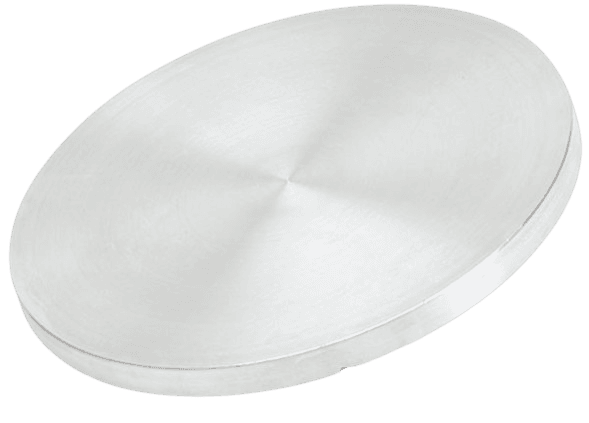
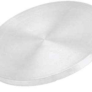
Barium Fluoride Sputtering Target Description
Barium Fluoride Sputtering Target from TFM is a fluoride ceramic material with the chemical formula BaF2.
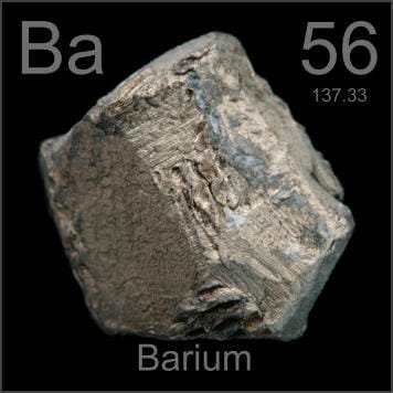 Barium, a soft and silvery alkaline earth metal, is the fifth element in group 2 of the periodic table. Due to its high reactivity, barium is not found in nature as a free element. Historically known as baryta, barium hydroxide doesn’t naturally occur as a mineral but can be produced by heating barium carbonate. The primary minerals containing barium are barite (barium sulfate, BaSO4) and witherite (barium carbonate, BaCO3), both of which are insoluble in water. The name “barium” is derived from the Greek word “barys,” meaning “heavy,” reflecting its high density.
Related Product: Barium Sputtering Target
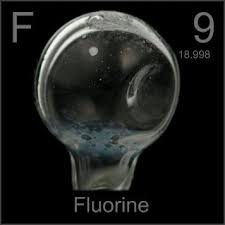 Fluorine, sometimes referred to as fluorin, is a chemical element whose name is derived from the Latin word ‘fluere,’ meaning ‘to flow.’ It was first noted in 1810 and observed by A.-M. Ampère. The element was later successfully isolated by H. Moissan. Fluorine is represented by the chemical symbol “F” and has an atomic number of 9 in the periodic table. It is located in Period 2 and Group 17, classified within the p-block. The relative atomic mass of fluorine is approximately 18.9984032(5) Dalton, with the number in brackets indicating the measurement uncertainty.
Barium Fluoride Sputtering Target Specification
| Compound Formula | BaF2 |
| Molecular Weight | 175.32 |
| Appearance | Solid |
| Melting Point | 1,291° C |
| Boiling Point | 2260° C |
| Density | 4.9 g/cm3 |
Barium Fluoride Sputtering Target Packaging
Our barium fluoride sputtering target is meticulously tagged and labeled externally for precise identification and quality control. We take great care in handling and packaging to prevent any damage during storage or transportation, ensuring the product’s integrity and quality are maintained upon arrival.
Get Contact
TFM offers Barium Fluoride Sputtering Targets in various forms, purities, sizes, and prices. We specialize in high-purity thin film deposition materials with optimal density and minimal grain sizes, which are ideal for semiconductor, CVD, and PVD applications in display and optics. Contact Us for current pricing on sputtering targets and other deposition materials that are not listed.


Reviews
There are no reviews yet.