 MSDS File
Introduction
Barium Strontium Titanate Evaporation Materials (Ba₀.₅Sr₀.₅TiO₃, commonly abbreviated as BST) are high-purity perovskite oxide source materials engineered for thin film deposition in tunable dielectric devices, microwave components, and advanced electronic systems. By combining barium titanate and strontium titanate in a controlled ratio, BST offers adjustable dielectric properties and temperature-dependent permittivity, making it highly suitable for functional thin film applications.
BST evaporation materials are specifically prepared for physical vapor deposition (PVD), including electron beam evaporation, enabling precise fabrication of dielectric and ferroelectric thin films.
Detailed Description
Ba₀.₅Sr₀.₅TiO₃ belongs to the ABO₃ perovskite family and exhibits a composition-dependent Curie temperature and dielectric constant. The 50:50 Ba/Sr ratio provides a balanced dielectric response, often used for tunable capacitor and RF device research.
Key characteristics of BST include:
High dielectric permittivity
Electric-field tunability
Low dielectric loss (when optimized)
Ferroelectric-to-paraelectric phase transition control
Strong compatibility with oxide substrates
BST Evaporation Materials are synthesized through controlled solid-state reactions of high-purity BaCO₃ (or BaO), SrCO₃ (or SrO), and TiO₂ precursors. After calcination and sintering, dense ceramic feedstock is produced to ensure compositional uniformity and stable evaporation behavior.
Because multi-component oxides can exhibit differential evaporation rates, material processing focuses on:
Precise stoichiometric control
High bulk density (typically ≥95% theoretical)
Homogeneous microstructure
Controlled grain size for stable melt behavior
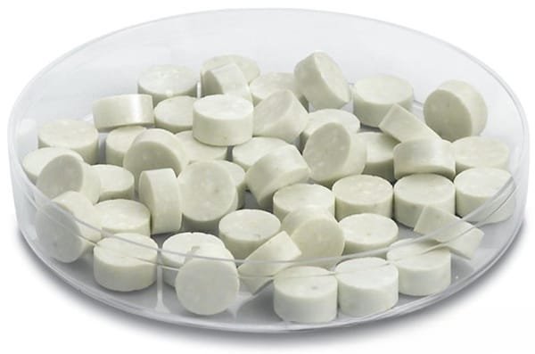
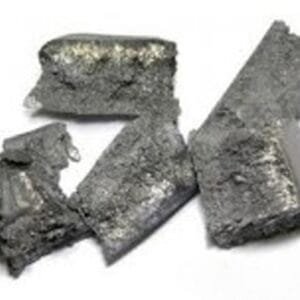
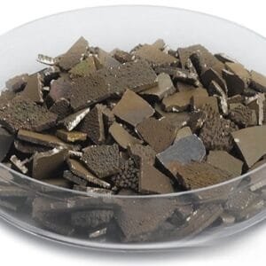
Available forms include:
Sintered pellets
Broken pieces or granules
Custom-shaped evaporation feedstock
These are compatible with electron beam evaporation systems commonly used in research and pilot-scale production.
Applications
Barium Strontium Titanate (BST) Evaporation Materials are widely used in:
Tunable microwave devices
RF phase shifters and filters
Dynamic random-access memory (DRAM) research
High-k dielectric thin films
Capacitors and varactors
Ferroelectric thin film devices
Electro-optic components
Advanced sensor systems
BST thin films are particularly valued in microwave electronics due to their electric-field-dependent permittivity, enabling voltage-controlled frequency tuning.
Technical Parameters
| Parameter | Typical Value / Range | Importance |
|---|---|---|
| Chemical Formula | Ba₀.₅Sr₀.₅TiO₃ | Defines dielectric behavior |
| Purity | 99.9% – 99.99% | Minimizes impurity phases |
| Density | ≥ 95% theoretical density | Stable evaporation & uniform films |
| Form | Pellets / Pieces / Granules | Compatible with evaporation systems |
| Deposition Method | Electron Beam Evaporation | Thin film fabrication |
| Dielectric Constant | Composition-dependent | Determines tunability |
| Curie Temperature | Adjustable via Ba/Sr ratio | Controls phase transition |
Comparison with Related Materials
| Material | Key Advantage | Typical Application |
|---|---|---|
| Ba₀.₅Sr₀.₅TiO₃ (BST) | Tunable dielectric constant | RF & microwave devices |
| BaTiO₃ | Strong ferroelectric behavior | Capacitors & actuators |
| SrTiO₃ | Quantum paraelectric behavior | Substrates & dielectric studies |
| Pb(Zr,Ti)O₃ (PZT) | High piezoelectric performance | Actuators & memory |
Compared with pure BaTiO₃, BST offers adjustable dielectric properties through Ba/Sr ratio tuning. Compared with PZT, BST avoids lead content and is preferred in certain environmentally sensitive applications.
FAQ
| Question | Answer |
|---|---|
| Can the Ba/Sr ratio be customized? | Yes, compositions can be tailored to achieve specific dielectric or phase transition characteristics. |
| Is BST suitable for electron beam evaporation? | Yes, high-density ceramic forms are optimized for stable e-beam deposition. |
| How is stoichiometry maintained during evaporation? | Material density and processing are controlled to reduce compositional deviation. |
| Can small R&D quantities be supplied? | Yes, flexible quantities are available for laboratory research. |
| How is it packaged? | Vacuum-sealed, moisture-protected packaging ensures material stability during transport. |
Packaging
Our Barium Strontium Titanate Evaporation Materials (Ba₀.₅Sr₀.₅TiO₃) are meticulously tagged and labeled externally to ensure efficient identification and maintain high standards of quality control. Each batch is carefully protected to prevent contamination and mechanical damage during storage and shipment.
Conclusion
Barium Strontium Titanate (Ba₀.₅Sr₀.₅TiO₃) Evaporation Materials provide a versatile and tunable dielectric solution for RF electronics, microwave components, and advanced thin film research. With controlled composition, high purity, and optimized ceramic density, BST supports reliable deposition of high-performance dielectric thin films.
For detailed specifications and a quotation, please contact us at sales@thinfilmmaterials.com.

Reviews
There are no reviews yet.